
实例介绍
【实例简介】RH850/E1L 用户手册:硬件
RH850/E1L User’s Manual: Hardware
【实例截图】


【核心代码】
Table of Contents
Section 1 Overview........................................................................................................ 47
1.1 Outline .......................................................................................................................................... 47
1.2 Features........................................................................................................................................ 49
1.3 Application Fields.......................................................................................................................... 53
1.4 Order Information.......................................................................................................................... 53
1.5 Pin Connection Diagram (Top View) ............................................................................................ 54
1.6 Functional Block Configuration..................................................................................................... 71
1.6.1 Internal Block Diagram ....................................................................................................... 71
Section 2 Pins................................................................................................................ 72
2.1 Port Functions............................................................................................................................... 72
2.1.1 Features ............................................................................................................................. 72
2.1.2 Overview............................................................................................................................. 73
2.1.2.1 Terms .................................................................................................................. 73
2.1.2.2 Overview of Pin Functions................................................................................... 74
2.1.2.3 Pin Data Input/Output.......................................................................................... 76
2.1.3 Port Type............................................................................................................................ 78
2.1.4 Port Group Configuration Register ..................................................................................... 80
2.1.4.1 Outline................................................................................................................. 80
2.1.4.2 Configuration of Pin Function.............................................................................. 82
2.1.4.3 Pin Data Input/Output.......................................................................................... 89
2.1.4.4 Configuration of Electrical Characteristics........................................................... 93
2.1.4.5 Port Register Protection ...................................................................................... 96
2.1.4.6 Pin-Unit Register ................................................................................................. 98
2.1.4.7 Example of Port Configuration Flow.................................................................. 100
2.1.5 Functional Selection ......................................................................................................... 105
2.1.5.1 Register Configuration in Use of the Alternative Function................................. 105
2.1.5.2 Alternative Function to be used in Direct I/O Control Alternative Mode ............ 105
2.1.5.3 Setting of the ERROROUT_C Pin..................................................................... 106
2.1.5.4 Register Setting in Use of an Analog Input Pin ................................................. 106
2.1.5.5 Register Setting in Use of the LVDS buffer....................................................... 107
2.1.5.6 Selecting of Function for JTAG Port.................................................................. 107
2.2 Organization of Port Groups....................................................................................................... 108
2.2.1 E1L Port Function............................................................................................................. 108
2.2.1.1 List of the E1L Port Registers............................................................................ 108
2.2.1.2 Alternative Function List of the E1L-BGA252 and QFP176 pins....................... 119
2.2.1.3 Alternative Function List of the E1L-QFP144 pins ............................................ 126
2.3 DNF ............................................................................................................................................ 131
2.3.1 Example of Noise Elimination........................................................................................... 131
2.3.2 Peripheral Function DNF.................................................................................................. 132
2.3.2.1 Overview of Peripheral Function DNF............................................................... 132
2.3.2.2 Details of the Control Registers......................................................................... 132
2.3.2.3 DNFP01nCTLm — Digital Noise Elimination Control Register ......................... 133
2.3.2.4 Setting Procedures of Peripheral Function DNF ............................................... 133
2.3.2.5 Peripheral Function Pin intended for DNF insertion.......................................... 134
2.3.3 Edge Detection DNF......................................................................................................... 135
2.3.3.1 Overview of the Function................................................................................... 135
2.3.3.2 Details of the Control Registers......................................................................... 135
2.3.3.3 DNFP02nCTL — Digital Noise Elimination Control Register ............................ 136
2.3.3.4 DNFP02nEDCm — Edge Detection Control Register....................................... 1372.3.3.5 DNFP02nEDFm — Edge Detection Flag Register............................................ 138
2.3.3.6 Setting Procedures of Edge Detection DNF...................................................... 138
2.3.3.7 Pn_m Pins Intended for DNF Insertion.............................................................. 139
2.4 POD Control ............................................................................................................................... 141
2.4.1 Overview of the Function.................................................................................................. 141
2.5 Pin Description............................................................................................................................ 143
2.5.1 Overview........................................................................................................................... 143
2.5.2 List of Pin Functions ......................................................................................................... 143
2.5.3 Pin State........................................................................................................................... 154
2.5.4 Handling of Unused Pins.................................................................................................. 156
Section 3 CPU System ................................................................................................ 160
3.1 Overview..................................................................................................................................... 160
3.1.1 Block Configuration .......................................................................................................... 160
3.2 CPU ............................................................................................................................................ 162
3.2.1 Core Functions ................................................................................................................. 162
3.2.1.1 Features ............................................................................................................ 162
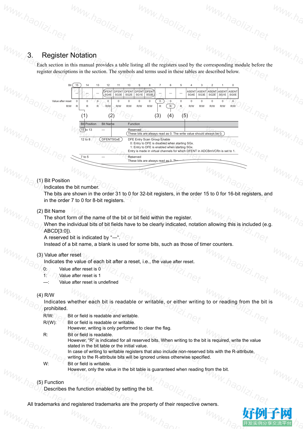
3.2.1.2 Register Set....................................................................................................... 163
3.2.2 Instruction Cache and Data Buffer ................................................................................... 202
3.2.2.1 Features ............................................................................................................ 202
3.2.2.2 Instruction Cache Function................................................................................ 203
3.2.2.3 Data Buffer Function ......................................................................................... 204
3.2.3 Inter-Processor Interrupts................................................................................................. 205
3.2.3.1 Inter-Processor Interrupt Control Registers....................................................... 205
3.2.4 Reliability Functions.......................................................................................................... 206
3.2.4.1 PE Guard Function (PEG)................................................................................. 206
3.2.4.2 PE’s Internal Peripheral Device Protection Function (IPG)............................... 211
3.2.4.3 System Error Notification Control Function (SEG) ............................................ 219
3.2.4.4 Checker Core .................................................................................................... 226
3.3 PCU ............................................................................................................................................ 227
3.3.1 Core Functions ................................................................................................................. 227
3.3.1.1 Features ............................................................................................................ 227
3.3.1.2 Register Set....................................................................................................... 228
3.3.2 Inter-Processor Interrupts................................................................................................. 256
3.3.3 Reliability Functions.......................................................................................................... 257
3.3.3.1 System Error Notification Control Function (SEG) ............................................ 257
3.4 Inter-CPU Functions ................................................................................................................... 260
3.4.1 Processor Element Identifier ............................................................................................ 260
3.4.2 Inter-Processor Interrupt Function.................................................................................... 260
3.4.3 Exclusive Function............................................................................................................ 260
3.4.3.1 Exclusive Control Register (MEV)..................................................................... 261
3.4.3.2 Operation of the LDL.W and STC.W Instructions.............................................. 262
3.5 Usage Notes............................................................................................................................... 264
3.5.1 Synchronization of Store Instruction Completion and Subsequent Instruction
Generation........................................................................................................................ 264
3.5.1.1 When updated results in the control registers are reflected in the
implementation of a subsequent instruction:..................................................... 264
3.5.1.2 When the updated results in the control registers and memories are
reflected in the instruction fetch of a subsequent instruction: ........................... 2653.5.1.3 When switching the code flash area.................................................................. 265
3.5.1.4 When executing the SYNCM instruction to wait for the completion of
update by the store instruction .......................................................................... 265
3.5.2 Accesses to Registers by Bit-Manipulation Instructions................................................... 266
3.5.3 Ensuring Coherency after Code Flash Programming....................................................... 266
3.5.4 Overwriting Context when Acknowledging Multiple Exceptions ....................................... 266
3.5.5 Usage Notes on Prefetching............................................................................................. 267
Section 4 Address Space............................................................................................. 268
4.1 Address Space ........................................................................................................................... 268
4.2 Address Space Viewed from Each Bus Master.......................................................................... 269
4.2.1 Space in which instructions can be fetched...................................................................... 269
4.2.2 Data space accessible by PE1......................................................................................... 269
4.2.3 Data space accessible by PCU ........................................................................................ 269
4.2.4 Data space accessible by DMA (DMAC, DTS)................................................................. 269
4.3 Global RAM and Retention RAM................................................................................................ 271
Section 5 Operating Mode ........................................................................................... 272
5.1 Features...................................................................................................................................... 272
5.2 Operating Mode.......................................................................................................................... 272
5.2.1 User Boot Mode................................................................................................................ 272
5.2.2 Serial Programming Mode................................................................................................ 272
5.2.3 Boundary Scan Mode....................................................................................................... 272
Section 6 Interrupt........................................................................................................ 273
6.1 Overview..................................................................................................................................... 273
6.2 Register Specifications ............................................................................................................... 275
6.2.1 Register Configuration...................................................................................................... 275
6.2.2 EIC0 to EIC511 — EI Level Interrupt Control Registers 0 to 511..................................... 277
6.2.3 IMR0 to IMR15 — EI Level Interrupt Mask Registers 0 to 15........................................... 279
6.2.4 EIBD0 to EIBD511 — EI Level Interrupt Bind Registers 0 to 511 .................................... 280
6.2.5 NMICTL — NMI Interrupt Control Register....................................................................... 281
6.2.6 EXINTCTL — External Interrupt Control Register............................................................ 282
6.2.7 EXINTSTR — External Interrupt Status Register............................................................. 283
6.2.8 EXINTSTC — External Interrupt Status Clear Register ................................................... 284
6.2.9 SINTR0 to SINTR3 — Software Interrupt Registers......................................................... 285
6.2.10 PINT0 to PINT7, PINTCLR0 to PINTCLR7 — Peripheral Interrupt Status Registers
and Peripheral Interrupt Status Clear Registers............................................................... 286
6.2.11 TIMER — Timer Interrupt Mask Enable Register............................................................. 290
6.3 Interrupt Sources ........................................................................................................................ 292
6.3.1 NMI Interrupts................................................................................................................... 292
6.3.2 IRQ Interrupts................................................................................................................... 292
6.3.3 ECM Interrupts ................................................................................................................. 292
6.3.4 Inter-Processor Interrupts................................................................................................. 292
6.3.5 Software Interrupts ........................................................................................................... 2936.3.6 On-Chip Peripheral Module Interrupts.............................................................................. 293
6.4 Interrupt Exception Handler and Priority Operations .................................................................. 294
6.5 Operation.................................................................................................................................... 308
6.5.1 External Interrupts (NMI/IRQ)........................................................................................... 308
6.5.2 Inter-Processor Interrupt................................................................................................... 308
6.5.3 Software Interrupt............................................................................................................. 308
6.5.4 DTS Interrupt Merge Function.......................................................................................... 308
6.5.5 ATU-IV/TSG2 Merge Function ......................................................................................... 309
6.5.6 Interrupt Processing Flow................................................................................................. 310
6.5.6.1 NMI Processing Flow ........................................................................................ 310
6.5.6.2 External Interrupt Processing Flow ................................................................... 311
6.5.6.3 Inter-Processor Interrupt Flow........................................................................... 313
6.5.6.4 Software Interrupt Processing Flow .................................................................. 314
6.5.6.5 DTS Interrupt Processing Flow ......................................................................... 316
6.6 Interrupt Response Times .......................................................................................................... 318
6.7 Using Interrupt Request Signals to Initiate Data Transfer .......................................................... 319
Section 7 DMA............................................................................................................. 320
7.1 Overview..................................................................................................................................... 320
7.1.1 Overview........................................................................................................................... 320
7.1.2 Term Definition ................................................................................................................. 321
7.2 DMA Function............................................................................................................................. 322
7.2.1 Basic Operation of DMA Transfer..................................................................................... 322
7.2.1.1 Transfer Mode................................................................................................... 322
7.2.1.2 Executing a DMA Cycle..................................................................................... 322
7.2.1.3 Updating Transfer Information........................................................................... 322
7.2.1.4 Last Transfer and Address Reload Transfer ..................................................... 323
7.2.1.5 Transfer Completion Interrupt and Transfer Count Match Interrupt Outputs..... 324
7.2.1.6 Continuous Transfer.......................................................................................... 324
7.2.2 Channel Priority Order...................................................................................................... 326
7.2.2.1 DMAC Channel Arbitration................................................................................ 326
7.2.2.2 DTS Channel Arbitration ................................................................................... 327
7.2.2.3 Interface Arbitration........................................................................................... 328
7.2.3 Reload Function ............................................................................................................... 329
7.2.3.1 Overview of the Reload Function ...................................................................... 329
7.2.3.2 Operation of Reload Function 1 ........................................................................ 329
7.2.3.3 Reload Function 2 ............................................................................................. 330
7.2.3.4 Timing of Setting DMAC Reload Registers ....................................................... 332
7.2.3.5 Timing of Setting DTS Reload Registers........................................................... 332
7.2.4 Chain Function ................................................................................................................. 333
7.2.4.1 Overview ........................................................................................................... 333
7.2.4.2 Setting Up the Chain Function .......................................................................... 334
7.2.4.3 Caution for Using the Chain Function ............................................................... 334
7.2.5 DMAC Operation .............................................................................................................. 335
7.2.5.1 Types of DMA Transfer Requests and Assigning DMA Transfer Requests...... 335
7.2.5.2 Generating and Accepting a Software DMA Transfer Request......................... 335
7.2.6 DTS Operation.................................................................................................................. 336
7.2.6.1 Types of DMA Transfer Requests and Assigning DMA Transfer Requests...... 336
7.2.6.2 Generating and Accepting a DMA Transfer Request........................................ 336
7.2.6.3 Executing DMA Transfer ................................................................................... 336
7.2.6.4 DTSRAM Access............................................................................................... 3377.3 Suspending, Resuming, and Aborting DMA Transfer and Clearing the DMA Transfer
Request ...................................................................................................................................... 338
7.3.1 Suspending and Resuming DMA Transfer by Software Control ...................................... 338
7.3.2 Suspending, Resuming, and Aborting Transfer by a DMAC Channel.............................. 338
7.3.3 Suspending, Resuming, and Aborting Transfer by the DTS............................................. 339
7.3.4 Masking and Clearing a Hardware DMA Transfer Request by the DTFR ........................ 341
7.3.5 Masking and Clearing a Hardware DMA Transfer Request by the DTSFSL.................... 341
7.3.6 List of Functions for Suspending, Resuming, and Aborting Transfer ............................... 342
7.4 Error Control ............................................................................................................................... 343
7.4.1 Type of Error..................................................................................................................... 343
7.4.2 DMA Transfer Error .......................................................................................................... 343
7.4.2.1 Operation of a DMAC When DMA Transfer Error Occurs................................. 343
7.4.2.2 Operation of a DTS When DMA Transfer Error Occurs .................................... 343
7.4.3 DTSRAM Error ................................................................................................................. 344
7.5 Reliability Function...................................................................................................................... 345
7.5.1 Overview........................................................................................................................... 345
7.5.2 Register Access Protection Function................................................................................ 345
7.5.2.1 Identifying the Accessing Master....................................................................... 345
7.5.2.2 Master Access................................................................................................... 345
7.5.2.3 Channel Assignment ......................................................................................... 345
7.5.2.4 Illegal Access .................................................................................................... 346
7.5.3 Master Information Inherit Function.................................................................................. 346
7.5.4 Other Reliability Functions................................................................................................ 347
7.5.4.1 Restriction on the Next Channel in the Chain ................................................... 347
7.6 Setting Up DMA Transfer............................................................................................................ 348
7.6.1 Overview of Setting Up DMA............................................................................................ 348
7.6.2 Setting Up the Overall DMA Operation............................................................................. 350
7.6.3 Setting Up the DMA Channel Setting ............................................................................... 350
7.6.3.1 Setting Up the DMAC Channel Setting ............................................................. 351
7.6.3.2 Setting Up the DTS Channel Setting................................................................. 352
7.7 DMA Trigger Source................................................................................................................... 353
7.7.1 List of DMA Trigger Sources ............................................................................................ 353
7.8 DTS Trigger Source.................................................................................................................... 357
7.8.1 List of DTS Trigger Sources ............................................................................................. 357
7.9 Global Register........................................................................................................................... 361
7.9.1 List of Global Register Addresses .................................................................................... 361
7.9.2 Details of Global Registers............................................................................................... 362
7.9.2.1 DMACTL — DMA Control Register................................................................... 362
7.9.2.2 DTSCTL1 — DTS Control Register 1................................................................ 363
7.9.2.3 DTSCTL2 — DTS Control Register 2................................................................ 364
7.9.2.4 DTSSTS — DTS Status Register...................................................................... 365
7.9.2.5 DMACER — DMAC Error Register ................................................................... 366
7.9.2.6 DTSER1 — DTS Error Register 1..................................................................... 367
7.9.2.7 DTSER2 — DTS Error Register 2..................................................................... 368
7.9.2.8 DTSERC — DTS Error Clear Register.............................................................. 369
7.9.2.9 DM0CMV — DMAC0 Register Access Protection Violation Register ............... 370
7.9.2.10 DTSCMV — DTS Register Access Protection Violation Register..................... 371
7.9.2.11 CMVC — Register Access Protection Violation Clear Register ........................ 372
7.9.2.12 DTSPRn — DTS Channel Priority Setting Register (n = 0 to 7)........................ 3737.9.2.13 DTRECCTL — DTSRAM ECC Control Register............................................... 377
7.9.2.14 DTRERINT — DTSRAM Error Notification Control Register............................. 378
7.9.2.15 DTRTSCTL — DTSRAM Test Control Register................................................ 379
7.9.2.16 DTRTWDAT — DTSRAM Test Write Data Register......................................... 380
7.9.2.17 DTRTRDAT — DTSRAM Test Read Data Register.......................................... 381
7.9.2.18 DMnnCM — DMAC Channel Master Setting Register (nn = 00 to 07) ............. 382
7.9.2.19 DTSnnnCM — DTS Channel Master Setting Register (nnn = 000 to 127) ....... 383
7.10 DMAC Channel Register ............................................................................................................ 385
7.10.1 DMAC Channel Register Address.................................................................................... 385
7.10.2 Details of DMAC Channel Registers ................................................................................ 386
7.10.2.1 DSAn — DMAC Source Address Register........................................................ 386
7.10.2.2 DDAn — DMAC Destination Address Register................................................. 387
7.10.2.3 DTCn — DMAC Transfer Count Register ......................................................... 388
7.10.2.4 DTCTn — DMAC Transfer Control Register ..................................................... 389
7.10.2.5 DRSAn — DMAC Reload Source Address Register......................................... 392
7.10.2.6 DRDAn — DMAC Reload Destination Address Register.................................. 393
7.10.2.7 DRTCn — DMAC Reload Transfer Count Register .......................................... 394
7.10.2.8 DTCCn — DMAC Transfer Count Compare Register....................................... 395
7.10.2.9 DCENn — DMAC Channel Operation Enable Setting Register........................ 396
7.10.2.10 DCSTn — DMAC Transfer Status Register ...................................................... 397
7.10.2.11 DCSTSn — DMAC Transfer Status Set Register.............................................. 399
7.10.2.12 DCSTCn — DMAC Transfer Status Clear Register .......................................... 400
7.10.2.13 DTFRn — DTFR Setting Register..................................................................... 401
7.10.2.14 DTFRRQn — DTFR Transfer Request Status Register.................................... 402
7.10.2.15 DTFRRQCn — DTFR Transfer Request Clear Register................................... 403
7.11 DTS Channel Register................................................................................................................ 404
7.11.1 Transfer information of the DTS (TI)................................................................................. 404
7.11.1.1 Structure of the TI.............................................................................................. 404
7.11.1.2 Organization of the TI in the DTSRAM.............................................................. 405
7.11.1.3 Accessing the TI................................................................................................ 406
7.11.1.4 Caution about accessing the TI......................................................................... 406
7.11.2 DTS Channel Register Address ....................................................................................... 407
7.11.3 Details of DTS Channel Registers.................................................................................... 408
7.11.3.1 DTSAnnn — DTS Source Address Register..................................................... 408
7.11.3.2 DTDAnnn — DTS Destination Address Register .............................................. 409
7.11.3.3 DTTCnnn — DTS Transfer Count Register....................................................... 410
7.11.3.4 DTTCTnnn — DTS Transfer Control Register .................................................. 411
7.11.3.5 DTRSAnnn — DTS Reload Source Address Register...................................... 414
7.11.3.6 DTRDAnnn — DTS Reload Destination Address Register ............................... 415
7.11.3.7 DTRTCnnn — DTS Reload Transfer Count Register........................................ 416
7.11.3.8 DTTCCnnn — DTS Transfer Count Compare Register .................................... 417
7.11.3.9 DTFSLnnn — DTSFSL Operation Setting Register .......................................... 418
7.11.3.10 DTFSTnnn — DTSFSL Transfer Request Status Register............................... 419
7.11.3.11 DTFSSnnn — DTSFSL Transfer Request Set Register.................................... 420
7.11.3.12 DTFSCnnn — DTSFSL Transfer Request Clear Register ................................ 420
Section 8 Resets.......................................................................................................... 421
8.1 Features...................................................................................................................................... 421
8.2 Reset State................................................................................................................................. 422
8.2.1 External Reset State......................................................................................................... 422
8.2.2 Internal Reset State.......................................................................................................... 422
8.3 Reset Sources ............................................................................................................................ 423
8.4 Register Specifications ............................................................................................................... 4248.4.1 List of Registers................................................................................................................ 424
8.4.2 RESF — Reset Source Determination Register............................................................... 425
8.4.3 RESFC — Reset Source Clear Register.......................................................................... 426
8.4.4 POF — Power-On Clear Flag Register ............................................................................ 427
8.4.5 POFC — Power-On Clear Flag Clear Register ................................................................ 427
8.4.6 SWRESA — Software Reset Request Register............................................................... 428
8.5 Software Reset ........................................................................................................................... 429
8.6 RAM Retention ........................................................................................................................... 429
8.7 Usage Notes............................................................................................................................... 429
Section 9 Power Supply Circuit.................................................................................... 430
9.1 Features...................................................................................................................................... 430
9.2 Example of Connection of Power Management IC..................................................................... 431
9.3 Power-on Sequence ................................................................................................................... 432
9.4 Usage Notes............................................................................................................................... 432
9.5 Guide to Mounting on Boards with an EPT................................................................................. 433
9.5.1 QFP .................................................................................................................................. 433
9.5.2 BGA.................................................................................................................................. 435
9.5.3 Reference Information...................................................................................................... 436
Section 10 Power Supply Voltage Monitor..................................................................... 437
10.1 Features...................................................................................................................................... 437
10.2 Configuration .............................................................................................................................. 437
10.3 Register Specifications ............................................................................................................... 438
10.3.1 DETFLG — CVM Detection Flag Register ....................................................................... 439
10.3.2 DETFLGC — CVM Detection Flag Clear Register........................................................... 440
10.3.3 VSCTL — CVM Control Register ..................................................................................... 441
10.3.4 HDETCTL — Upper Limit Voltage Setting Register ......................................................... 442
10.3.5 LDETCTL — Lower Limit Voltage Register...................................................................... 443
10.3.6 VSDETFCTL — Detection Signal Filter Control Register................................................. 444
10.4 Usage ......................................................................................................................................... 445
10.5 Notes on Usage.......................................................................................................................... 447
Section 11 Clock Controller ........................................................................................... 448
11.1 Features...................................................................................................................................... 448
11.2 Type of Clocks............................................................................................................................ 449
11.3 Input/Output Pins........................................................................................................................ 451
11.3.1 How to Connect a Crystal Resonator ............................................................................... 451
11.4 Register Specification................................................................................................................. 452
11.4.1 List of Registers................................................................................................................ 452
11.4.2 PLL0CLKS — PLL0 Status Register ................................................................................ 453
11.4.3 PLL0CLKC1 — PLL0 Control Register 1.......................................................................... 454
11.4.4 CKSC0CTL — Clock 0 Selection Control Register .......................................................... 456
11.4.5 CKSC0ACT — Clock 0 Selection Active Register............................................................ 45711.4.6 CLKD0DIV — Clock 0 Division Register .......................................................................... 458
11.4.7 CLKD0STAT — Clock 0 Division Status Register............................................................ 459
11.4.8 CKSC1CTL — Clock 1 Selection Control Register .......................................................... 460
11.4.9 CKSC1ACT — Clock 1 Selection Active Register............................................................ 461
11.4.10 PROT1PHCMD — Protect 1 Command Register ............................................................ 462
11.4.11 PROT1PS — Protect 1 Status Register ........................................................................... 464
11.5 Operation.................................................................................................................................... 465
11.5.1 Operation When the Divide Function Is Used .................................................................. 465
11.6 Notes .......................................................................................................................................... 468
11.6.1 Board Design Notes ......................................................................................................... 468
11.7 ASIC Clock ................................................................................................................................. 469
11.7.1 Features ........................................................................................................................... 469
11.7.2 Configuration .................................................................................................................... 469
11.7.3 Register Specifications..................................................................................................... 470
11.7.3.1 ACK0CKC — Clock Control Register................................................................ 471
11.7.3.2 ACK0CKCFLG — CKC Flag Register............................................................... 472
11.7.3.3 ACK0CKCTL — Clock Select Register ............................................................. 473
11.7.3.4 ACK0BRGA0CMP — BRGA0 Compare Register............................................. 474
11.7.3.5 ACK0CKCPCMD — CKC Protect Command Register ..................................... 475
11.7.3.6 ACK0CKCPS — CKC Protect Status Register ................................................. 477
11.7.4 Usage ............................................................................................................................... 478
11.7.4.1 CK Pin Output Function..................................................................................... 478
11.7.4.2 CK Output Baud Rate Generator Circuit (BRGA).............................................. 478
11.7.4.3 Control Register Rewrite Protect....................................................................... 479
11.7.4.4 CK Output Switching Procedure........................................................................ 480
Section 12 Standby Controller ....................................................................................... 482
12.1 Features...................................................................................................................................... 482
12.1.1 Types of Power-Down Mode ............................................................................................ 482
12.2 Operation.................................................................................................................................... 483
12.2.1 Power Off Standby Mode ................................................................................................. 483
12.2.2 Module Standby Function................................................................................................. 483
12.3 Register List................................................................................................................................ 484
12.3.1 List of Registers................................................................................................................ 484
12.3.2 EPTCNT — EPT Control Register.................................................................................... 485
12.3.3 PROT0PHCMD — Protection Command Register........................................................... 486
12.3.4 PROT0PS — Protection Command Status Register........................................................ 488
12.3.5 Module Standby Registers ............................................................................................... 489
12.3.5.1 MSRTSG — Module Standby Register – TSG2................................................ 489
12.3.5.2 MSRTAPA — Module Standby Register – TAPA.............................................. 490
12.3.5.3 MSROSTM — Module Standby Register – OSTM............................................ 491
12.3.5.4 MSRWDTA — Module Standby Register – WDTA ........................................... 491
12.3.5.5 MSRPIC — Module Standby Register – PIC .................................................... 492
12.3.5.6 MSRRCAN — Module Standby Register – RS-CAN ........................................ 492
12.3.5.7 MSRRLIN — Module Standby Register – RLIN2.............................................. 493
12.3.5.8 MSRSCI — Module Standby Register – SCI3 .................................................. 494
12.3.5.9 MSRCSIH — Module Standby Register – CSIH ............................................... 495
12.3.5.10 MSRSAD — Module Standby Register – SAR AD............................................ 496
12.3.5.11 MSRDAD — Module Standby Register – ΔΣAD ............................................... 49612.3.5.12 MSRATU — Module Standby Register – ATU-IV ............................................. 497
12.3.5.13 MSRAPA — Module Standby Register – APA.................................................. 497
12.3.5.14 MSRDFE — Module Standby Register – DFE.................................................. 498
12.3.5.15 MSRRHSB — Module Standby Register – RHSB ............................................ 499
12.3.6 MSRPCMD — MSR Protection Command Register ........................................................ 500
12.3.7 MSRPS — MSR Protection Status Register .................................................................... 502
Section 13 Clocked Serial Interface H (CSIH) ............................................................... 503
13.1 CSIH Features............................................................................................................................ 503
13.2 Notes on Pin Combination.......................................................................................................... 505
13.3 Function Overview...................................................................................................................... 506
13.4 List of the Usage Notes .............................................................................................................. 508
13.5 Functional Description ................................................................................................................ 510
13.5.1 Operating Modes (master/slave) ...................................................................................... 511
13.5.2 Master/Slave Connections................................................................................................ 513
13.5.3 Chip Selection (CS) Features........................................................................................... 515
13.5.4 Chip Select Timing Details ............................................................................................... 518
13.5.5 Transmission Clock Selection .......................................................................................... 521
13.5.6 Data transfer modes......................................................................................................... 523
13.5.7 Data Length Selection ...................................................................................................... 524
13.5.8 Serial Data Direction Selection......................................................................................... 527
13.5.9 Communication in Slave Mode......................................................................................... 528
13.5.10 CSIH interrupt requests.................................................................................................... 531
13.5.11 Handshake function.......................................................................................................... 538
13.5.12 Error Detection ................................................................................................................. 540
13.5.13 Loop-Back Mode .............................................................................................................. 544
13.5.14 Enforced Chip Select Idle Setting..................................................................................... 545
13.6 CSIH Control Registers .............................................................................................................. 546
13.6.1 CSIHnCTL0 — CSIH Control Register 0.......................................................................... 547
13.6.2 CSIHnCTL1 — CSIH Control Register 1.......................................................................... 548
13.6.3 CSIHnCTL2 — CSIH Control Register 2.......................................................................... 551
13.6.4 CSIHnSTR0 — CSIH Status Register 0 ........................................................................... 553
13.6.5 CSIHnSTCR0 — CSIH Status Clear Register 0............................................................... 555
13.6.6 CSIHnCFGx — CSIH Configuration Register x................................................................ 556
13.6.7 CSIHnTX0W — CSIH Transmit Data Register 0 for Word Access .................................. 561
13.6.8 CSIHnTX0H — CSIH Transmit Data Register 0 for Half Word Access............................ 563
13.6.9 CSIHnRX0W — CSIH Receive Data Register 0 for Word Access ................................... 564
13.6.10 CSIHnRX0H — CSIH Receive Data Register 0 for Half Word Access ............................ 565
13.6.11 CSIHnBRSi — CSIHn Baud Rate Setting Register i ........................................................ 566
13.7 Operating Procedures................................................................................................................. 567
13.7.1 Procedures in Direct Access Mode .................................................................................. 567
Section 14 Serial Communication Interface 3 (SCI3) .................................................... 571
14.1 Overview..................................................................................................................................... 571
14.1.1 Features of SCI3 .............................................................................................................. 57114.1.2 Outline of Functions.......................................................................................................... 571
14.1.3 Serial Communication Modes........................................................................................... 572
14.1.4 Block Diagram .................................................................................................................. 572
14.2 Input/Output Pins........................................................................................................................ 573
14.3 Register Descriptions.................................................................................................................. 574
14.3.1 SCI3nRSR — Receive Shift Register............................................................................... 575
14.3.2 SCI3nRDR — Receive Data Register .............................................................................. 575
14.3.3 SCI3nTDR — Transmit Data Register.............................................................................. 575
14.3.4 SCI3nTSR — Transmit Shift Register .............................................................................. 575
14.3.5 SCI3nSMR — Serial Mode Register ................................................................................ 576
14.3.6 SCI3nSCR — Serial Control Register .............................................................................. 577
14.3.7 SCI3nSSR — Serial Status Register................................................................................ 579
14.3.8 SCI3nSCMR — Serial Transfer Format Register............................................................. 581
14.3.9 SCI3nSEMR — Serial Extended Mode Register.............................................................. 582
14.3.10 SCI3nBRR — Bit Rate Register ....................................................................................... 583
14.3.11 SCI3nMDDR — Modulation Duty Register....................................................................... 586
14.4 Operation in Asynchronous Mode .............................................................................................. 587
14.4.1 Transmission/Receive Format.......................................................................................... 588
14.4.2 Receive Data Sampling Timing and Receive Margin ....................................................... 589
14.4.3 Clock................................................................................................................................. 590
14.4.4 Double-Speed Operation.................................................................................................. 590
14.4.5 SCI3 Initialization (Asynchronous Mode).......................................................................... 591
14.4.6 Serial Data Transmission (Asynchronous Mode) ............................................................. 592
14.4.7 Serial Data Receive (Asynchronous Mode)...................................................................... 595
14.5 Multi-Processor Communication Function.................................................................................. 599
14.5.1 Overview and Sample Connection ................................................................................... 599
14.5.2 Multi-Processor Serial Data Transmission ....................................................................... 600
14.5.3 Multi-Processor Serial Data Receive................................................................................ 601
14.6 Operation in Clock Synchronous Mode ...................................................................................... 605
14.6.1 Clock................................................................................................................................. 605
14.6.2 SCI3 Initialization (Clock Synchronous Mode) ................................................................. 606
14.6.3 Serial Data Transmission (Clock Synchronous Mode)..................................................... 607
14.6.4 Serial Data Receive (Clock Synchronous Mode) ............................................................. 610
14.6.5 Simultaneous Serial Data Transmission and Reception (Clock Synchronous Mode) ...... 612
14.7
Bit Rate Modulation Function...................................................................................................... 614
14.8 Interrupt Sources ........................................................................................................................ 615
14.9 Usage Notes............................................................................................................................... 616
14.9.1 Break Detection and Processing ...................................................................................... 616
14.9.2 Mark State and Break Output........................................................................................... 616
14.9.3 Receive Error Flags and Transmit Operations in Clock Synchronous Mode ................... 616
14.9.4 Relationship between Writing to SCI3nTDR and the TDRE Flag..................................... 616
14.9.5 Restrictions on Using an External Clock for Transmission in Clock Synchronous
Mode................................................................................................................................. 617
14.9.6 External Clock Input in Clock Synchronous Mode............................................................ 617Section 15 LIN Master Interface (RLIN2)....................................................................... 618
15.1 Overview of RH850/E1L RLIN2.................................................................................................. 618
15.1.1 Units and Channels .......................................................................................................... 618
15.1.2 Register Base Addresses................................................................................................. 618
15.1.3 Clock Supply..................................................................................................................... 619
15.1.4 Interrupt Request.............................................................................................................. 619
15.1.5 Reset Sources.................................................................................................................. 619
15.1.6 External Input/Output Signals........................................................................................... 619
15.2 Function...................................................................................................................................... 620
15.2.1 Functional Overview......................................................................................................... 620
15.2.2 Block Diagram .................................................................................................................. 621
15.3 Registers..................................................................................................................................... 622
15.3.1 List of Registers................................................................................................................ 622
15.3.2 Global Registers............................................................................................................... 623
15.3.2.1 RLN21nGLWBR — LIN Wake-up Baud Rate Select Register.......................... 623
15.3.2.2 RLN21nGLBRP0 — LIN Baud Rate Prescaler 0 Register ................................ 624
15.3.2.3 RLN21nGLBRP1 — LIN Baud Rate Prescaler 1 Register ................................ 625
15.3.2.4 RLN21nGLSTC — LIN Self-Test Control Register............................................ 626
15.3.3 Channel Registers............................................................................................................ 627
15.3.3.1 RLN21nmLiMD — LIN Mode Register .............................................................. 627
15.3.3.2 RLN21nmLiBFC — LIN Break Field Configuration Register............................. 628
15.3.3.3 RLN21nmLiSC — LIN Space Configuration Register ....................................... 629
15.3.3.4 RLN21nmLiWUP — LIN Wake-up Configuration Register................................ 630
15.3.3.5 RLN21nmLiIE — LIN Interrupt Enable Register................................................ 631
15.3.3.6 RLN21nmLiEDE — LIN Error Detection Enable Register................................. 632
15.3.3.7 RLN21nmLiCUC — LIN Control Register ......................................................... 634
15.3.3.8 RLN21nmLiTRC — LIN Transmission Control Register ................................... 635
15.3.3.9 RLN21nmLiMST — LIN Mode Status Register................................................. 636
15.3.3.10 RLN21nmLiST — LIN Status Register.............................................................. 637
15.3.3.11 RLN21nmLiEST — LIN Error Status Register................................................... 639
15.3.3.12 RLN21nmLiDFC — LIN Data Field Configuration Register............................... 641
15.3.3.13 RLN21nmLiIDB — LIN ID Buffer Register......................................................... 643
15.3.3.14 RLN21nmLiCBR — LIN Checksum Buffer Register.......................................... 644
15.3.3.15 RLN21nmLiDBRb — LIN Data Buffer b Register.............................................. 645
15.4 Interrupt Sources ........................................................................................................................ 646
15.5 Modes......................................................................................................................................... 647
15.6 LIN Reset Mode.......................................................................................................................... 649
15.7 LIN Operation Mode ................................................................................................................... 650
15.8 LIN Wake-up Mode..................................................................................................................... 650
15.9 Header Transmission/Response Transmission/Response Reception........................................ 651
15.9.1 Header Transmission ....................................................................................................... 651
15.9.2 Response Transmission................................................................................................... 652
15.9.3 Response Reception ........................................................................................................ 653
15.10 Data Transmission/Reception..................................................................................................... 654
15.10.1 Data Transmission............................................................................................................ 654
15.10.2 Data Reception................................................................................................................. 655
15.11 Transmit/Receive Data Buffering................................................................................................ 656
15.11.1 Transmission of LIN Frames ............................................................................................ 65615.11.2 Reception of LIN Frames.................................................................................................. 657
15.12 Wake-up Transmission/Reception.............................................................................................. 658
15.12.1 Wake-up Transmission..................................................................................................... 658
15.12.2 Wake-up Reception.......................................................................................................... 659
15.12.3 Wakeup Collision.............................................................................................................. 659
15.13 Status.......................................................................................................................................... 660
15.14 Error Status................................................................................................................................. 661
15.14.1 Types of Error Status........................................................................................................ 661
15.14.2 Target Time Area for Error Detection ............................................................................... 662
15.15 LIN Self-Test Mode..................................................................................................................... 663
15.15.1 Change to LIN Self-Test Mode......................................................................................... 664
15.15.2 Transmission in LIN Self-Test Mode ................................................................................ 665
15.15.3 Reception in LIN Self-Test Mode...................................................................................... 666
15.15.4 Terminating LIN Self-Test Mode....................................................................................... 668
15.16 Baud Rate Generator.................................................................................................................. 669
Section 16 CAN Interface (RS-CAN) ............................................................................. 671
16.1 Overview of RS-CAN.................................................................................................................. 671
16.1.1 Number of Units................................................................................................................ 671
16.1.2 Register Base Address..................................................................................................... 671
16.1.3 Clock Supply..................................................................................................................... 672
16.1.4 Interrupt and DMA / DTS.................................................................................................. 672
16.1.5 Reset Sources.................................................................................................................. 673
16.1.6 External I/O Signals.......................................................................................................... 673
16.2 Overview..................................................................................................................................... 674
16.2.1 Functional Outline............................................................................................................. 674
16.2.2 Block Diagram .................................................................................................................. 676
16.3 Register Descriptions.................................................................................................................. 677
16.3.1 Register List...................................................................................................................... 677
16.3.2 Register Details ................................................................................................................ 700
16.3.2.1 RSCAN0CmCFG — Channel Configuration Register (m = 0 to 3) ................... 700
16.3.2.2 RSCAN0CmCTR — Channel Control Register (m = 0 to 3) ............................. 702
16.3.2.3 RSCAN0CmSTS — Channel Status Register (m = 0 to 3) ............................... 706
16.3.2.4 RSCAN0CmERFL — Channel Error Flag Register (m = 0 to 3)....................... 708
16.3.2.5 RSCAN0GCFG — Global Configuration Register............................................. 712
16.3.2.6 RSCAN0GCTR — Global Control Register....................................................... 715
16.3.2.7 RSCAN0GSTS — Global Status Register ........................................................ 717
16.3.2.8 RSCAN0GERFL — Global Error Flag Register ................................................ 719
16.3.2.9 RSCAN0GTINTSTS0 — Global TX Interrupt Status Register 0 ....................... 720
16.3.2.10 RSCAN0GTSC — Global Timestamp Counter Register................................... 723
16.3.2.11 RSCAN0GAFLECTR — Receive Rule Entry Control Register ......................... 724
16.3.2.12 RSCAN0GAFLCFG0 — Receive Rule Configuration Register 0...................... 725
16.3.2.13 RSCAN0GAFLIDj — Receive Rule ID Register (j = 0 to 15)............................. 727
16.3.2.14 RSCAN0GAFLMj — Receive Rule Mask Register (j = 0 to 15) ........................ 728
16.3.2.15 RSCAN0GAFLP0j — Receive Rule Pointer 0 Register (j = 0 to 15) ................. 729
16.3.2.16 RSCAN0GAFLP1j — Receive Rule Pointer 1 Register (j = 0 to 15) ................. 731
16.3.2.17 RSCAN0RMNB — Receive Buffer Number Register........................................ 732
16.3.2.18 RSCAN0RMNDy — Receive Buffer New Data Register y (y = 0, 1)................. 73316.3.2.19 RSCAN0RMIDq — Receive Buffer ID Register (q = 0 to 63)............................ 734
16.3.2.20 RSCAN0RMPTRq — Receive Buffer Pointer Register (q = 0 to 63) ................ 735
16.3.2.21 RSCAN0RMDF0q — Receive Buffer Data Field 0 Register (q = 0 to 63)......... 736
16.3.2.22 RSCAN0RMDF1q — Receive Buffer Data Field 1 Register (q = 0 to 63)......... 737
16.3.2.23 RSCAN0RFCCx — Receive FIFO Buffer Configuration/Control Register
(x = 0 to 7)......................................................................................................... 738
16.3.2.24 RSCAN0RFSTSx — Receive FIFO Buffer Status Register (x = 0 to 7)............ 740
16.3.2.25 RSCAN0RFPCTRx — Receive FIFO Buffer Pointer Control Register
(x = 0 to 7)......................................................................................................... 742
16.3.2.26 RSCAN0RFIDx — Receive FIFO Buffer Access ID Register (x = 0 to 7) ......... 743
16.3.2.27 RSCAN0RFPTRx — Receive FIFO Buffer Access Pointer Register
(x = 0 to 7)......................................................................................................... 744
16.3.2.28 RSCAN0RFDF0x — Receive FIFO Buffer Access Data Field 0 Register
(x = 0 to 7)......................................................................................................... 745
16.3.2.29 RSCAN0RFDF1x — Receive FIFO Buffer Access Data Field 1 Register
(x = 0 to 7)......................................................................................................... 746
16.3.2.30 RSCAN0CFCCk — Transmit/Receive FIFO Buffer Configuration/
Control Register (k = 0 to 11)............................................................................ 747
16.3.2.31 RSCAN0CFSTSk — Transmit/Receive FIFO Buffer Status Register
(k = 0 to 11)....................................................................................................... 751
16.3.2.32 RSCAN0CFPCTRk — Transmit/Receive FIFO Buffer Pointer Control
Register (k = 0 to 11)......................................................................................... 754
16.3.2.33 RSCAN0CFIDk — Transmit/Receive FIFO Buffer Access ID Register
(k = 0 to 11)....................................................................................................... 756
16.3.2.34 RSCAN0CFPTRk — Transmit/Receive FIFO Buffer Access Pointer Register
(k = 0 to 11)....................................................................................................... 758
16.3.2.35 RSCAN0CFDF0k — Transmit/Receive FIFO Buffer Access Data Field 0
Register (k = 0 to 11)......................................................................................... 760
16.3.2.36 RSCAN0CFDF1k — Transmit/Receive FIFO Buffer Access Data Field 1
Register (k = 0 to 11)......................................................................................... 761
16.3.2.37 RSCAN0FESTS — FIFO Empty Status Register.............................................. 762
16.3.2.38 RSCAN0FFSTS — FIFO Full Status Register .................................................. 764
16.3.2.39 RSCAN0FMSTS — FIFO Message Lost Status Register................................. 766
16.3.2.40 RSCAN0RFISTS — Receive FIFO Buffer Interrupt Flag Status Register......... 768
16.3.2.41 RSCAN0CFRISTS — Transmit/Receive FIFO Buffer Reception Interrupt
Flag Status Register.......................................................................................... 769
16.3.2.42 RSCAN0CFTISTS — Transmit/Receive FIFO Buffer Transmission Interrupt
Flag Status Register.......................................................................................... 770
16.3.2.43 RSCAN0TMCp — Transmit Buffer Control Register (p = 0 to 63) .................... 771
16.3.2.44 RSCAN0TMSTSp — Transmit Buffer Status Register (p = 0 to 63) ................. 773
16.3.2.45 RSCAN0TMTRSTSy — Transmit Buffer Transmit Request Status Register y
(y = 0, 1)............................................................................................................ 775
16.3.2.46 RSCAN0TMTARSTSy — Transmit Buffer Transmit Abort Request Status
Register (y = 0, 1).............................................................................................. 777
16.3.2.47 RSCAN0TMTCSTSy — Transmit Buffer Transmit Complete Status Register
(y = 0, 1)............................................................................................................ 779
16.3.2.48 RSCAN0TMTASTSy — Transmit Buffer Transmit Abort Status Register
(y = 0, 1)............................................................................................................ 781
16.3.2.49 RSCAN0TMIECy — Transmit Buffer Interrupt Enable Configuration Register
(y = 0, 1)............................................................................................................ 783
16.3.2.50 RSCAN0TMIDp — Transmit Buffer ID Register (p = 0 to 63) ........................... 785
16.3.2.51 RSCAN0TMPTRp — Transmit Buffer Pointer Register (p = 0 to 63)................ 786
16.3.2.52 RSCAN0TMDF0p — Transmit Buffer Data Field 0 Register (p = 0 to 63) ........ 787
16.3.2.53 RSCAN0TMDF1p — Transmit Buffer Data Field 1 Register (p = 0 to 63) ........ 788
16.3.2.54 RSCAN0TXQCCm — Transmit Queue Configuration/Control Register
(m = 0 to 3)........................................................................................................ 789
16.3.2.55 RSCAN0TXQSTSm — Transmit Queue Status Register (m = 0 to 3).............. 79116.3.2.56 RSCAN0TXQPCTRm — Transmit Queue Pointer Control Register
(m = 0 to 3)........................................................................................................ 793
16.3.2.57 RSCAN0THLCCm — Transmit History List Configuration/Control Register
(m = 0 to 3)........................................................................................................ 794
16.3.2.58 RSCAN0THLSTSm — Transmit History List Status Register (m = 0 to 3) ....... 796
16.3.2.59 RSCAN0THLACCm — Transmit History List Access Register (m = 0 to 3) ..... 798
16.3.2.60 RSCAN0THLPCTRm — Transmit History List Pointer Control Register
(m = 0 to 3)........................................................................................................ 799
16.3.2.61 RSCAN0GTSTCFG — Global Test Configuration Register.............................. 800
16.3.2.62 RSCAN0GTSTCTR — Global Test Control Register........................................ 802
16.3.2.63 RSCAN0GLOCKK — Global Lock Key Register............................................... 803
16.3.2.64 RSCAN0RPGACCr — RAM Test Page Access Register (r = 0 to 63) ............. 804
16.4 Functions .................................................................................................................................... 805
16.4.1 Interrupt Sources.............................................................................................................. 805
16.4.2 CAN Modes ...................................................................................................................... 809
16.4.2.1 Global Modes .................................................................................................... 809
16.4.2.2 Global Stop Mode.............................................................................................. 810
16.4.2.3 Global Reset Mode............................................................................................ 810
16.4.2.4 Global Test Mode.............................................................................................. 811
16.4.2.5 Global Operating Mode ..................................................................................... 811
16.4.2.6 Channel Modes ................................................................................................. 812
16.4.2.7 Channel Stop Mode........................................................................................... 813
16.4.2.8 Channel Reset Mode......................................................................................... 813
16.4.2.9 Channel Halt Mode............................................................................................ 814
16.4.2.10 Channel Communication Mode......................................................................... 814
16.4.2.11 Bus Off State..................................................................................................... 815
16.4.3 Function for Reception ..................................................................................................... 817
16.4.3.1 Data Processing Using the Receive Rule Table ............................................... 817
16.4.3.2 Acceptance Filter Processing............................................................................ 819
16.4.3.3 DLC Filter Processing ....................................................................................... 819
16.4.3.4 Routing Processing ........................................................................................... 820
16.4.3.5 Label Addition Processing................................................................................. 820
16.4.3.6 Mirror Function Processing ............................................................................... 820
16.4.3.7 Timestamp......................................................................................................... 820
16.4.4 Transmission Functions.................................................................................................... 822
16.4.4.1 Transmit Priority Determination......................................................................... 823
16.4.4.2 Transmission Using Transmit Buffers ............................................................... 823
16.4.4.3 Transmit Abort Function.................................................................................... 823
16.4.4.4 One-Shot Transmission Function (Retransmission Disabling Function)........... 824
16.4.4.5 Transmission Using FIFO Buffers ..................................................................... 824
16.4.4.6 Interval Transmission Function ......................................................................... 824
16.4.4.7 Transmission Using Transmit Queues .............................................................. 826
16.4.4.8 Transmit History Function ................................................................................. 827
16.4.5 Gateway Function............................................................................................................. 828
16.4.6 Test Function.................................................................................................................... 829
16.4.6.1 Standard Test Mode.......................................................................................... 829
16.4.6.2 Listen-Only Mode .............................................................................................. 829
16.4.6.3 Self-Test Mode (Loopback Mode)..................................................................... 830
16.4.6.4 Self-Test Mode 0 (External Loopback Mode).................................................... 830
16.4.6.5 Self-Test Mode 1 (Internal Loopback Mode)..................................................... 830
16.4.6.6 RAM Test .......................................................................................................... 831
16.4.6.7 Inter-Channel Communication Test................................................................... 831
16.5 Procedures ................................................................................................................................. 832
16.5.1 Initial Settings ................................................................................................................... 832
16.5.1.1 Clock Setting ..................................................................................................... 83316.5.1.2 Bit Timing Setting .............................................................................................. 834
16.5.1.3 Communication Speed Setting.......................................................................... 835
16.5.1.4 Receive Rule Setting......................................................................................... 836
16.5.1.5 Buffer Setting..................................................................................................... 837
16.5.2 Procedure for Reception................................................................................................... 839
16.5.2.1 Receive Buffer Reading Procedure................................................................... 839
16.5.2.2 FIFO Buffer Reading Procedure........................................................................ 841
16.5.3 Transmission Procedure................................................................................................... 844
16.5.3.1 Procedure for Transmission from Transmit Buffers........................................... 844
16.5.3.2 Procedure for Transmission from Transmit/Receive FIFO Buffers ................... 848
16.5.3.3 Procedure for Transmission from the Transmit Queue ..................................... 852
16.5.3.4 Transmit History Buffer Reading Procedure...................................................... 852
16.5.4 Test Settings..................................................................................................................... 853
16.5.4.1 Self-Test Mode Setting Procedure .................................................................... 853
16.5.4.2 Procedure for Releasing the Protection ............................................................ 854
16.5.4.3 RAM Test Setting Procedure............................................................................. 855
16.5.4.4 Inter-Channel Communication Test Setting Procedure..................................... 856
16.6 Notes on the RS-CAN Module.................................................................................................... 857
Section 17 FlexRay........................................................................................................ 858
Section 18 Renesas High-Speed Bus (RHSB) .............................................................. 859
18.1 Overview..................................................................................................................................... 859
18.1.1 Features of RHSB ............................................................................................................ 859
18.1.2 Module Overview.............................................................................................................. 860
18.1.2.1 Downstream Channel Communication Functions ............................................. 860
18.1.2.2 Upstream Channel Communication Functions.................................................. 861
18.1.2.3 Interrupts ........................................................................................................... 861
18.1.2.4 DMA Support..................................................................................................... 861
18.1.2.5 Other Features .................................................................................................. 861
18.1.2.6 Caution.............................................................................................................. 861
18.1.3 Block Diagram .................................................................................................................. 862
18.2 Register Descriptions.................................................................................................................. 863
18.2.1 I/O Registers Overview..................................................................................................... 863
18.2.2 Legend.............................................................................................................................. 864
18.2.3 Description of the Registers in the Common Controller ................................................... 865
18.2.3.1 RHSBjGC — Global Configuration Register ..................................................... 865
18.2.3.2 RHSBjMSR — Module Status Register............................................................. 867
18.2.4 Downstream (Tx) Registers.............................................................................................. 869
18.2.4.1 RHSBjDCR — Downstream Configuration Register ......................................... 869
18.2.4.2 RHSBjDCR1 — Downstream Configuration Register for Period 1.................... 872
18.2.4.3 RHSBjDEC — Data Element Configuration Register........................................ 873
18.2.4.4 RHSBjSDCi — Slave Device Configuration Register i (i = 0)............................ 875
18.2.4.5 RHSBjDEBAm — Data Element Bit Assignment Register m (m = 0 to 3) ........ 877
18.2.4.6 RHSBjEBEi — Emergency Bit Enable Register i (i = 0, 1)................................ 879
18.2.4.7 RHSBjDTC — Downstream Transmission Control Register............................. 880
18.2.4.8 RHSBjDCD — Downstream Command Data Register ..................................... 882
18.2.4.9 RHSBjDDRi — Downstream Data Register i (i = 0, 1) ...................................... 883
18.2.4.10 iRHSBjDEDi — Downstream Emergency Data Register (i = 0, 1) .................... 884
18.2.5 Upstream (Rx) Registers.................................................................................................. 885
18.2.5.1 RHSBjUCR — Upstream Configuration Register.............................................. 885
18.2.5.2 RHSBjUCC — Upstream Channel Configuration Register ............................... 887
18.2.5.3 RHSBjUCS — Upstream Channel Selection Register ...................................... 89018.2.5.4 RHSBjUDR — Upstream Data Read Register.................................................. 892
18.2.5.5 RHSBjUDi — Upstream Data Register i (i = 0, 1) ............................................. 895
18.2.5.6 RHSBjUSS — Upstream Status Summary Register......................................... 898
18.2.6 Interrupt Registers............................................................................................................ 900
18.2.6.1 RHSBjIC — Interrupt Control Register.............................................................. 900
18.2.6.2 RHSBjIS — Interrupt Status Register................................................................ 902
18.3 Operation States......................................................................................................................... 907
18.3.1 Operation State Description ............................................................................................. 907
18.3.1.1 RESET State..................................................................................................... 907
18.3.1.2 CONFIG State................................................................................................... 907
18.3.1.3 ACTIVE State.................................................................................................... 907
18.3.1.4 TEST State........................................................................................................ 908
18.3.2 Activation of the RHSB Module (Leaving RESET State).................................................. 908
18.3.3 Deactivation of the RHSB Module (Entering RESET State)............................................. 909
18.3.4 Changing between Operation States (ACTIVE, CONFIG, TEST).................................... 909
18.3.5 Leaving ACTIVE State without Interrupting Ongoing Transmission................................. 910
18.4 RHSB operations........................................................................................................................ 911
18.4.1 Downstream Communication ........................................................................................... 911
18.4.1.1 Downstream Communication Phases ............................................................... 912
18.4.1.2 Frame Dependent Flagging............................................................................... 914
18.4.1.3 Downstream Modes .......................................................................................... 915
18.4.1.4 Command Frame Insertion Methods in Multi-Period Repetition Mode.............. 922
18.4.1.5 Physical Frame Format ..................................................................................... 924
18.4.1.6 Data Frame Assembling.................................................................................... 926
18.4.1.7 Command Frame Assembling........................................................................... 928
18.4.1.8 Emergency Function ......................................................................................... 929
18.4.1.9 Downstream Bit Rates....................................................................................... 931
18.4.1.10 Data Update and Data Frame Transmission Request ...................................... 932
18.4.1.11 Command Frame Transmission Request.......................................................... 933
18.4.2 Upstream Communication................................................................................................ 933
18.4.2.1 Upstream Modes............................................................................................... 935
18.4.2.2 Individual Slave Configuration........................................................................... 935
18.4.2.3 Frame Format Types......................................................................................... 937
18.4.2.4 Frame Storing.................................................................................................... 938
18.4.2.5 Upstream Bit Rates ........................................................................................... 938
18.4.2.6 Update of Decoding Status ............................................................................... 939
18.4.3 Timeout Detection ............................................................................................................ 940
18.4.3.1 Command Transmission with Remote Data Request ....................................... 941
18.4.3.2 Timeout Detection Details ................................................................................. 942
18.4.4 Test Mode Operation........................................................................................................ 943
18.4.4.1 Test Mode Data Generation.............................................................................. 944
18.5 Interrupts..................................................................................................................................... 945
18.5.1 Downstream Related Interrupts (Transmission)............................................................... 945
18.5.2 Upstream Related Interrupts (Reception)......................................................................... 945
18.5.3 Interrupt Request Details.................................................................................................. 946
18.6 DMA Capability........................................................................................................................... 947
18.6.1 DMA Usage for Downstream Data Transmission............................................................. 947
18.6.1.1 Configuring and Enabling Flow to Use Downstream data DMA........................ 947
18.6.1.2 Data Layout in Memory for Downstream Data DMA ......................................... 948
18.6.2 DMA Usage for Downstream Command Transmission.................................................... 948
18.6.2.1 Configuring and Enabling Flow to Use Downstream Command DMA .............. 948
18.6.2.2 Command Data Layout in Memory for Downstream Command DMA............... 94918.6.3 DMA Usage for Upstream Data Reception....................................................................... 950
18.6.3.1 Configuring and Enabling Flow to Use Upstream DMA .................................... 950
18.6.3.2 Data Layout in Memory for Upstream DMA ...................................................... 950
18.7 Cross Bar (XBAR)....................................................................................................................... 951
18.7.1 Overview........................................................................................................................... 951
18.7.2 Module Configuration ....................................................................................................... 951
18.7.2.1 RHSB XBAR Configuration ............................................................................... 951
18.7.3 Register Specifications..................................................................................................... 952
18.7.3.1 List of Registers................................................................................................. 952
18.7.3.2 RHSBGiCRjH — Microsecond Bus Control Register H .................................... 953
18.7.3.3 RHSBGiCRjL — Microsecond Bus Control Register L...................................... 957
18.7.4 Summary of Operation ..................................................................................................... 961
Section 19 Window Watchdog Timer (WDTA)............................................................... 962
19.1 Features...................................................................................................................................... 962
19.2 Overview..................................................................................................................................... 963
19.2.1 Functional Overview......................................................................................................... 963
19.2.2 Block Diagram .................................................................................................................. 963
19.3 Registers..................................................................................................................................... 964
19.3.1 Registers Overview .......................................................................................................... 964
19.3.1.1 WDTAnWDTE — WDTA Enable Register ........................................................ 965
19.3.1.2 WDTAnMD — WDTA Mode Register................................................................ 966
19.4 Interrupt Sources ........................................................................................................................ 967
19.5 Functional Description ................................................................................................................ 968
19.5.1 WDTA after Reset Release .............................................................................................. 968
19.5.1.1 Start modes....................................................................................................... 968
19.5.1.2 Start mode selection (only for WDTA0)............................................................. 968
19.5.1.3 WDTA settings after reset release .................................................................... 968
19.5.1.4 Default start mode timing (only for WDTA0)...................................................... 969
19.5.1.5 Software trigger start mode timing (common to WDTA0 and WDTA1)............. 970
19.5.2 WDTA Trigger................................................................................................................... 971
19.5.3 Error Detection ................................................................................................................. 971
19.5.4 WDTA Error Mode............................................................................................................ 972
19.5.5 75% Interrupt Request Signals......................................................................................... 973
19.5.6 Window Function.............................................................................................................. 974
Section 20 OS Timer (OSTM)........................................................................................ 975
20.1 Functional Overview ................................................................................................................... 975
20.1.1 Features ........................................................................................................................... 975
20.2 Registers..................................................................................................................................... 976
20.2.1 Registers Overview .......................................................................................................... 976
20.2.2 Details of OSTM Registers............................................................................................... 977
20.2.2.1 OSTMnCMP — OSTM Compare Register........................................................ 977
20.2.2.2 OSTMnCNT — OSTM Counter Register .......................................................... 978
20.2.2.3 OSTMnTO — OSTM Output Register............................................................... 979
20.2.2.4 OSTMnTOE — OSTM Output Enable Register ................................................ 979
20.2.2.5 OSTMnTE — OSTM Count Enable Status Register......................................... 980
20.2.2.6 OSTMnTS — OSTM Count Start Trigger Register ........................................... 98120.2.2.7 OSTMnTT — OSTM Count Stop Trigger Register............................................ 981
20.2.2.8 OSTMnCTL — OSTM Control Register ........................................................... 982
20.3 Functional Description ................................................................................................................ 983
20.3.1 Block Diagram .................................................................................................................. 983
20.3.2 Counter Clock................................................................................................................... 983
20.3.3 Output Modes (only for OSTM0) ...................................................................................... 984
20.3.4 Interrupt Request Generation........................................................................................... 985
20.3.5 Starting and Stopping the Timer....................................................................................... 986
20.3.6 Interval Timer Mode.......................................................................................................... 988
20.3.6.1 Basic Operation in Interval Timer Mode............................................................ 988
20.3.6.2 Operation when OSTMnCMP = 0000 0000H.................................................... 991
20.3.7 Free-Running Comparison Mode ..................................................................................... 992
20.3.7.1 Basic Operation in Free-Running Comparison Mode........................................ 992
20.3.7.2 Operation when OSTMnCMP = 0000 0000H...................................................................994
Section 21 Advanced Timer Unit IV (ATU-IV)................................................................ 995
21.1 Overview..................................................................................................................................... 995
21.1.1 Configuration of ATU-IV ................................................................................................... 999
21.1.2 ATU-IV Registers............................................................................................................ 1001
21.1.3 ATU-IV Input/Output Signals .......................................................................................... 1032
21.1.4 Clock Supply................................................................................................................... 1034
21.2 Common Controller................................................................................................................... 1035
21.2.1 Operation........................................................................................................................ 1035
21.2.2 Register Description of Common Controller................................................................... 1036
21.2.2.1 ATUENR — ATU-IV Master Enable Register.................................................. 1036
21.2.2.2 CBCNT — Clock Bus Control Register ........................................................... 1039
21.2.2.3 NCMR — Noise Cancellation Mode Register.................................................. 1040
21.3 Prescaler................................................................................................................................... 1046
21.3.1 Operation........................................................................................................................ 1046
21.3.2 Register Description of Prescalers ................................................................................. 1047
21.3.2.1 PSCRx — Prescaler Registers x (x = 0 to 3) .................................................. 1047
21.3.3 Details of Operation........................................................................................................ 1048
21.3.3.1 Starting Prescalers.......................................................................................... 1048
21.3.3.2 Stopping and Restarting Operation................................................................. 1048
21.4 Timer A ..................................................................................................................................... 1049
21.4.1 Operation........................................................................................................................ 1049
21.4.2 Timer A Control Registers .............................................................................................. 1051
21.4.2.1 TCR1A — Timer Control Register 1A ............................................................. 1051
21.4.2.2 TCR2A — Timer Control Register 2A ............................................................. 1053
21.4.2.3 TCR3A — Timer Control Register 3A ............................................................. 1054
21.4.2.4 TCR4A — Timer Control Register 4A ............................................................. 1055
21.4.2.5 NCMCR1A — Noise Cancellation Mode Channel Register 1A....................... 1056
21.4.2.6 NCMCR2A — Noise Cancellation Mode Channel Register 2A....................... 1059
21.4.2.7 TIOR1A — Timer I/O Control Register 1A ...................................................... 1062
21.4.2.8 TIOR2A — Timer I/O Control Register 2A ...................................................... 1064
21.4.2.9 TSRA — Timer Status Register A................................................................... 1067
21.4.2.10 TSCRA — Timer Status Clear Register A....................................................... 1069
21.4.2.11 ICRAx — Input Capture Registers Ax (x = 0 to 5)........................................... 1071
21.4.2.12 TCNTA — Free-Running Counter A................................................................ 1072
21.4.2.13 TILRA — Timer Input Signal Level Register A................................................ 107321.4.2.14 TILCRA — Timer Input Signal Level Capture Register A................................ 1074
21.4.2.15 NCNTAx — Noise Canceler Counters Ax (x = 0 to 5)..................................... 1075
21.4.2.16 NCRAx — Noise Canceler Registers Ax (x = 0 to 5) ...................................... 1077
21.4.3 Detailed Operation.......................................................................................................... 1079
21.4.3.1 Operation of Noise Canceler........................................................................... 1079
21.4.3.2 Operation of Free-Running Counter................................................................ 1082
21.4.3.3 Input Capture................................................................................................... 1083
21.4.3.4 Pin Level Capture Operation........................................................................... 1085
21.4.3.5 DMA Transfer.................................................................................................. 1085
21.5 Timer B ..................................................................................................................................... 1086
21.5.1 Operation........................................................................................................................ 1086
21.5.2 Timer B Control Registers .............................................................................................. 1089
21.5.2.1 TCRB — Timer Control Register B ................................................................. 1089
21.5.2.2 TIORB — Timer I/O Control Register B .......................................................... 1091
21.5.2.3 TSRB — Timer Status Register B................................................................... 1093
21.5.2.4 TSCRB — Timer Status Clear Register B....................................................... 1097
21.5.2.5 TICRB — Timer Interrupt Control Register B.................................................. 1099
21.5.2.6 TCNTB0 — Edge Interval Measuring Counter B0........................................... 1101
21.5.2.7 ICRB0 — Input Capture Register B0............................................................... 1102
21.5.2.8 RECRBx— Record Registers Bx (x = 1 to 6) .................................................. 1103
21.5.2.9 RBURBx — Record Backup Registers Bx ( x = 0 to 6) ................................... 1104
21.5.2.10 ICRB3x — Input Capture Registers B3x (x = 0 to 6)....................................... 1105
21.5.2.11 OCRB0 — Output Compare Register B0........................................................ 1106
21.5.2.12 TCNTB1 — Event Counter B1 ........................................................................ 1107
21.5.2.13 OCRB1 — Output Compare Register B1........................................................ 1108
21.5.2.14 OCRB10 — Output Compare Register B10.................................................... 1109
21.5.2.15 OCRB11 — Output Compare Register B11.................................................... 1110
21.5.2.16 OCRB12 — Output Compare Register B12.................................................... 1111
21.5.2.17 ICRB1 — Input Capture Register B1............................................................... 1112
21.5.2.18 ICRB2 — Input Capture Register B2............................................................... 1113
21.5.2.19 LDB — Load Register B.................................................................................. 1114
21.5.2.20 RLDB — Reload Register B............................................................................ 1115
21.5.2.21 TCNTB2 — Reload Counter B2 ...................................................................... 1116
21.5.2.22 PIMR1 — Pulse Interval Multiplier Register 1 ................................................. 1117
21.5.2.23 PIMR2 — Pulse Interval Multiplier Register 2 ................................................. 1118
21.5.2.24 TCNTB6 — Multiplied Clock Counter B6 ........................................................ 1119
21.5.2.25 ICRB6 — Input Capture Register B6............................................................... 1120
21.5.2.26 RARB6 — Multiplication Setting Register B6.................................................. 1121
21.5.2.27 TCNTB6M — Frequency-Multiplied Clock Counter B6M ................................ 1122
21.5.2.28 OCRB6 — Output Compare Register B6........................................................ 1123
21.5.2.29 OCRB7 — Output Compare Register B7........................................................ 1124
21.5.2.30 TCNTB3 — Correcting Event Counter B3....................................................... 1125
21.5.2.31 OCRB8 — Output Compare Register B8........................................................ 1126
21.5.2.32 TCNTB4 — Multiplied-and-Corrected Clock Counter B4 ................................ 1127
21.5.2.33 TCNTB5 — Multiplied-and-Corrected Clock Generating Counter B5 ............. 1128
21.5.2.34 TCCLFRB — Correcting Counter Clear Flag Register B ................................ 1129
21.5.2.35 TCCLFSRB — Correcting Counter Clear Flag Setting Register B.................. 1130
21.5.2.36 TCCLFCRB — Correcting Counter Clear Flag Clearing Register B ............... 1131
21.5.2.37 TCCLRB — Correcting Counter Clearing Register B...................................... 1132
21.5.2.38 ACRTRGB — AGCKM2 Correction Enable Setting Register.......................... 1133
21.5.2.39 ACRCLRB — AGCKM2 Correction Clear Setting Register............................. 1134
21.5.2.40 ACRSTRB — AGCKM2 Correction Status Register ....................................... 1135
21.5.2.41 ACRVALRB — AGCKM2 Correction Clock Count Setting Register ............... 1136
21.5.3 Detailed Operation.......................................................................................................... 1137
21.5.3.1 Edge Interval Measuring Function and Edge Input Stopping Function ........... 1137
21.5.3.2 Frequency-Multiplied Clock Generator............................................................ 114021.5.3.3 Frequency-Multiplied Clock Signal Corrector.................................................. 1144
21.6 Timer C..................................................................................................................................... 1151
21.6.1 Operation........................................................................................................................ 1151
21.6.2 Timer C Registers........................................................................................................... 1153
21.6.2.1 TSTRC — Timer Start Register C................................................................... 1153
21.6.2.2 NCCRCx — Noise Canceler Control Register Cx (x = 0 to 5)......................... 1155
21.6.2.3 TCRCx — Timer Control Registers C (x = 0 to 5) ........................................... 1158
21.6.2.4 TSRCx — Timer Status Registers Cx (x = 0 to 5)........................................... 1162
21.6.2.5 TSCRCx — Timer Status Clear Register Cx (x = 0 to 5) ................................ 1165
21.6.2.6 TIORCx — Timer I/O Control Registers Cx (x = 0 to 5) .................................. 1167
21.6.2.7 TCNTCx — Timer Counters Cx (x = 0 to 5) .................................................... 1170
21.6.2.8 GRCxy — General Registers Cxy................................................................... 1171
21.6.2.9 NCNTCxy — Noise Canceler Counters Cxy ................................................... 1173
21.6.2.10 NCRCxy — Noise Canceler Registers Cxy..................................................... 1175
21.6.2.11 OCRCxy — Output Compare Registers Cxy................................................... 1176
21.6.2.12 TIERCx — Timer Interrupt Enable Registers Cx............................................. 1177
21.6.2.13 CUCRCx — Counter Upper-Limit Setting Compare Registers Cx.................. 1178
21.6.2.14 NCMCR1C — Noise Cancellation Mode Channel Register 1C ...................... 1179
21.6.2.15 NCMCR2C — Noise Cancellation Mode Channel Register 2C ...................... 1182
21.6.3 Operation........................................................................................................................ 1185
21.6.3.1 Input Capture Mode — Input Capture Function .............................................. 1185
21.6.3.2 Compare Match Mode — Compare Match Function....................................... 1187
21.6.3.3 PWM Function................................................................................................. 1189
21.6.3.4 One-Shot Pulse Mode — One-Shot Pulse Function ....................................... 1190
21.6.3.5 Counter Upper-Limit Setting Function............................................................. 1197
21.7 Timer D..................................................................................................................................... 1200
21.7.1 Operation Overview........................................................................................................ 1200
21.7.2 Registers Related to Timer D ......................................................................................... 1202
21.7.2.1 TSTRD — Timer Start Register D................................................................... 1202
21.7.2.2 TCRDx — Timer Control Registers Dx............................................................ 1204
21.7.2.3 TIOR1Dx — Timer I/O Control Registers 1Dx................................................. 1208
21.7.2.4 TIOR2Dx — Timer I/O Control Register 2Dx .................................................. 1210
21.7.2.5 OSELRDx — Line Select Register Dx............................................................. 1211
21.7.2.6 ODRDx — Output Value Register Dx.............................................................. 1212
21.7.2.7 DSTRDx — Down Counter Start Register Dx ................................................. 1213
21.7.2.8 DSR1Dx — Down Counter Status Registers 1Dx........................................... 1214
21.7.2.9 DSR2Dx — Down Count Status Register 2Dx................................................ 1216
21.7.2.10 DSCRDx — Down Count Status Clear Register Dx........................................ 1217
21.7.2.11 DCRDx — Down Counter Control Registers Dx ............................................. 1218
21.7.2.12
TSRDx — Timer Status Registers Dx ............................................................. 1220
21.7.2.13 TSCRDx — Timer Status Clear Register Dx................................................... 1224
21.7.2.14 TOCRDx — Timer Output Control Registers Dx............................................. 1226
21.7.2.15 OSBRDx — Timer Offset Base Registers Dx.................................................. 1227
21.7.2.16 TICTSELDx — Timer Input Capture Trigger Select Register Dx .................... 1228
21.7.2.17 TCNT1Dx — Timer Counter 1Dx .................................................................... 1229
21.7.2.18 TCNT2Dx — Timer Counter 2Dx .................................................................... 1230
21.7.2.19 CUCR1Dx — Counter Upper-Limit Setting Compare Register 1Dx................ 1231
21.7.2.20 CUCR2Dx — Counter Upper-Limit Setting Compare Register 2Dx................ 1232
21.7.2.21 OCR1Dxy — Output Compare Registers 1Dxy............................................... 1233
21.7.2.22 RCR1Dx — Range Comparison Value Setting Register 1Dx ......................... 1234
21.7.2.23 OCR2Dxy — Output Compare Registers 2Dxy............................................... 1236
21.7.2.24 RCR2Dx — Range Comparison Value Setting Register 2Dx ......................... 1237
21.7.2.25 ICR1Dxy — Input capture register 1Dxy ......................................................... 1239
21.7.2.26 ICR2Dxy — Input capture register 2Dxy ......................................................... 1240
21.7.2.27 DCNTDxy — Timer Down Counters Dxy ........................................................ 124121.7.3 Operation........................................................................................................................ 1243
21.7.3.1 Range Comparison Function........................................................................... 1248
21.7.3.2 Counter Upper-Limit Setting Function............................................................. 1249
21.7.3.3 Capture Function............................................................................................. 1250
21.8 Timer E ..................................................................................................................................... 1252
21.8.1 Operation Overview........................................................................................................ 1252
21.8.2 Registers Related to Timer E ......................................................................................... 1254
21.8.2.1 TSTRE — Timer Start Register E ................................................................... 1254
21.8.2.2 SSTREx — Subblock Starting Registers Ex ................................................... 1255
21.8.2.3 PSCREx — Prescaler Registers Ex................................................................ 1257
21.8.2.4 PSCCRExy — Prescaler Channel Registers Exy ........................................... 1258
21.8.2.5 TCREx — Timer Control Register Ex.............................................................. 1259
21.8.2.6 RLDCREx — Reload Control Registers Ex..................................................... 1260
21.8.2.7 POECREx — Output Shutoff Control Register Ex .......................................... 1261
21.8.2.8 SOLVLEx — Output Shutoff Level Setting Register Ex .................................. 1262
21.8.2.9 TSREx — Timer Status Registers E ............................................................... 1263
21.8.2.10 TSCREx — Timer Status Clear Register Ex ................................................... 1265
21.8.2.11 TIEREx — Timer Interrupt Enable Registers Ex ............................................. 1267
21.8.2.12 TOCREx — Timer Output Control Registers Ex ............................................. 1269
21.8.2.13 TCNTExy — Timer Counters Exy ................................................................... 1270
21.8.2.14 CYLRExy — Cycle-Setting Registers Exy....................................................... 1271
21.8.2.15 DTRExy — Duty Cycle Setting Registers Exy................................................. 1272
21.8.2.16 CRLDExy — Cycle Reload Registers Exy ...................................................... 1273
21.8.2.17 DRLDExy — Duty Cycle Reload Registers Exy.............................................. 1274
21.8.3 Operation Description..................................................................................................... 1275
21.9 Timer F ..................................................................................................................................... 1280
21.9.1 Operation Overview........................................................................................................ 1280
21.9.2 Registers Related to Timer F.......................................................................................... 1282
21.9.2.1 TSTRF — Timer Start Register F.................................................................... 1282
21.9.2.2 NCMCR1F — Noise Cancellation Mode Channel Register 1F ....................... 1284
21.9.2.3 NCMCR2F — Noise Cancellation Mode Channel Register 2F ....................... 1286
21.9.2.4 NCCRF — Noise Canceller Control Register F............................................... 1288
21.9.2.5 PVFCRF — Private Function Control Register F ............................................ 1290
21.9.2.6 TCR1Fx — Timer Control Registers 1Fx ........................................................ 1291
21.9.2.7 TCR2Fx — Timer Control Registers 2Fx ........................................................ 1293
21.9.2.8 TIERFx — Timer Interrupt Enable Registers Fx.............................................. 1294
21.9.2.9 BKCRFx — Backup Control Register Fx......................................................... 1296
21.9.2.10 TSRFx — Timer Status Registers Fx.............................................................. 1298
21.9.2.11 TSCRFx — Timer Status Clear Register Fx.................................................... 1300
21.9.2.12 ECNTAFx — Timer Measurement Counters AFx ........................................... 1302
21.9.2.13 ECNTBFx — Event Counters Fx..................................................................... 1303
21.9.2.14 ECNTCFx — Time measurement Counters CFx ............................................ 1304
21.9.2.15 GRAFx — General Registers AFx................................................................... 1305
21.9.2.16 BGRAFx — Backup Register AFx................................................................... 1306
21.9.2.17 GRBFx — General Registers BFx................................................................... 1307
21.9.2.18 GRCFx — General Registers CFx .................................................................. 1308
21.9.2.19 BGRCFx — Backup Register CFx .................................................................. 1309
21.9.2.20 GRDFx — General Registers DFx .................................................................. 1310
21.9.2.21 BGRDFx — Backup Register DFx .................................................................. 1311
21.9.2.22 CDRFx — Capture Output Registers Fx ......................................................... 1312
21.9.2.23 NCNTFAx — Noise Canceler Counters FAx................................................... 1314
21.9.2.24 NCNTFBx — Noise Canceler Counters FBx................................................... 1316
21.9.2.25 NCRFAx — Noise Cancel Registers FAx........................................................ 1318
21.9.2.26 NCRFBx — Noise Cancel Registers FBx........................................................ 131921.9.3 Detailed Operation Description....................................................................................... 1320
21.9.3.1 Edge Counting in a Given Time ...................................................................... 1320
21.9.3.2 Effective Edge Interval Counting..................................................................... 1322
21.9.3.3 Measurement of Time during High/Low Input Levels...................................... 1324
21.9.3.4 Measurement of PWM Input Waveform Timing .............................................. 1326
21.9.3.5 Rotation Speed/Pulse Measurement............................................................... 1329
21.9.3.6 Up/Down Event Count..................................................................................... 1331
21.9.3.7 Four-time Multiplication Event Count .............................................................. 1333
21.9.3.8 Overflow and Underflow.................................................................................. 1335
21.9.3.9 Simultaneous Access of Multiple Registers .................................................... 1335
21.10 Timer G..................................................................................................................................... 1336
21.10.1 Operation Overview........................................................................................................ 1336
21.10.2 Registers Related to Timer G......................................................................................... 1337
21.10.2.1 TSTRG — Timer Start Register G................................................................... 1337
21.10.2.2 TCRGx — Timer Control Register Gx............................................................. 1338
21.10.2.3 TSRGx — Timer Status Registers Gx............................................................. 1339
21.10.2.4 TSCRGx — Timer Status Clear Register Gx .................................................. 1341
21.10.2.5 TCNTGx — Timer Counters Gx ...................................................................... 1342
21.10.2.6 OCRGx — Compare Match Registers Gx....................................................... 1343
21.10.3 Detailed Operation Description....................................................................................... 1344
21.11 Timer H..................................................................................................................................... 1345
21.11.1 Operation Overview........................................................................................................ 1345
21.11.2 Registers Related to Timer H ......................................................................................... 1346
21.11.2.1 TCRH — Timer Control Register H................................................................. 1346
21.11.2.2 TSRH — Timer Status Register H................................................................... 1347
21.11.2.3 TSCRH — Timer Status Clear Register H ...................................................... 1349
21.11.2.4 TCNT1H — Timer Counter 1H........................................................................ 1350
21.11.2.5 OCR1H — Compare Match Register 1H......................................................... 1351
21.11.2.6 TCNT2H — Timer Counter 2H........................................................................ 1352
21.11.3 Operation Description..................................................................................................... 1353
21.12 Timer J...................................................................................................................................... 1354
21.12.1 Operation Overview........................................................................................................ 1354
21.12.2 Registers Related to Timer J.......................................................................................... 1355
21.12.2.1 TSTRJ — Timer Start Register J..................................................................... 1355
21.12.2.2 TCRJx — Timer Control Registers Jx ............................................................. 1356
21.12.2.3 FCRJx — FIFO Control Registers Jx .............................................................. 1358
21.12.2.4 TSRJx — Timer Status Register Jx................................................................. 1360
21.12.2.5 TSCRJx — Timer Status Clear Register Jx .................................................... 1363
21.12.2.6
TCNTJx — Timer Counter Jx.......................................................................... 1365
21.12.2.7 OCRJx — Compare Match Registers Jx......................................................... 1366
21.12.2.8 FIFOJx — FIFO Registers Jx.......................................................................... 1367
21.12.2.9 FDNRJx — FIFO Data Count Registers Jx..................................................... 1368
21.12.2.10 NCNTJx — Noise Canceler Counters Jx ........................................................ 1369
21.12.2.11 NCRJx — Noise Cancel Registers Jx ............................................................. 1371
21.12.3 Operation description ..................................................................................................... 1372
21.13 Automatic Switching of DMA and AD Requests ....................................................................... 1375
21.13.1 Overview of Operation.................................................................................................... 1375
21.13.2 DMA/AD Requests Auto-Switching Registers ................................................................ 1376
21.13.2.1 TRGSRDMA0 — Trigger Status Register DMA0 ............................................ 1376
21.13.2.2 TRGSELDMA00 — Trigger Select Register DMA00....................................... 1377
21.13.2.3 TRGSELDMA01 — Trigger Select Register DMA01....................................... 1378
21.13.2.4 TRGSELAD — Trigger Select Register AD..................................................... 1379
21.13.2.5 TRGSRDMA1 — Trigger Status Register DMA1 ............................................ 137921.13.2.6 TRGSELDMA10 — Trigger Select Register DMA10....................................... 1380
21.13.2.7 TRGSELDMA11 — Trigger Select Register DMA11....................................... 1381
21.13.3 Details of Operation........................................................................................................ 1382
21.13.3.1 Data DMA Trigger ........................................................................................... 1382
21.13.3.2 Count DMA Trigger ......................................................................................... 1383
21.13.3.3 SAR-AD Trigger .............................................................................................. 1384
21.14 Usage Notes............................................................................................................................. 1385
21.14.1 Input Capture Contention ............................................................................................... 1385
21.14.1.1 Contention between Writing to General Register and Input Capture .............. 1385
21.14.1.2 Contention between Writing to Counter and Input Capture............................. 1386
21.14.1.3 Contention between Setting and Clearing of Input Capture Status Flag......... 1387
21.14.2 Compare Match Contention............................................................................................ 1388
21.14.2.1 Contention between Writing to Compare-Match General Register and
Compare Match............................................................................................... 1388
21.14.2.2 Contention between Writing to CYLRExy and Cycle Match of TCNTExy ....... 1389
21.14.2.3 Contention between Writing to DTRExy and Cycle Match of TCNTExy ......... 1389
21.14.2.4 Contention between Writing to Counter and Compare Match......................... 1390
21.14.2.5 Contention between Writing to Counter and Counter Clearing by
Compare Match............................................................................................... 1391
21.14.2.6 Contention between Writing to TCNTExy and Counter Clearing by
Cycle Match .................................................................................................... 1392
21.14.2.7 Contention between Setting and Clearing of Compare Match Status Flag..... 1393
21.14.2.8 Contention between Setting of Cycle Match Status Flag and Writing 1 to the
Status Clear Register ...................................................................................... 1394
21.14.2.9 Contention between Detection of 1H Compare Match and Disabling of
Counter by ATUENR Setting........................................................................... 1395
21.14.2.10 Contention between Writing 0 to TCNTExy and Cycle Match......................... 1396
21.14.3 Load/Reload Contention................................................................................................. 1397
21.14.3.1 Contention between Data Transfer and Writing to Transfer Destination
Register........................................................................................................... 1397
21.14.3.2 Contention between Data Transfer and Writing to Transfer Source
Register........................................................................................................... 1398
21.14.4 Counter Contention ........................................................................................................ 1399
21.14.4.1 Contention between Writing to Counter and Count-Up/Count-Down.............. 1399
21.14.4.2 Contention between Count-Up and Counter Clearing..................................... 1399
21.14.4.3 Contention between Writing to Counter and Overflow .................................... 1400
21.14.4.4 Contention between Setting and Clearing of Overflow Status Flag ................ 1401
21.14.4.5 Contention between Overflow and Counter Clearing by Compare Match....... 1402
21.14.5 Contention in Noise Canceler......................................................................................... 1404
21.14.5.1
Contention between Writing to Noise Canceler Counter and
Compare Match with Noise Canceler Register ............................................... 1404
21.14.5.2 Contention between Writing to Noise Canceler Register and
Compare Match with Noise Canceler Counter................................................ 1405
21.14.6 Contention in Timer Down Counter Dxy......................................................................... 1406
21.14.6.1 Contention between Writing to DCNTDxy Counter and Count-Down ............. 1406
21.14.6.2 Contention between Writing to DCNTDxy Counter and Underflow................. 1406
21.14.6.3 Counter Stop Trigger — Contention between Writing to DCNTDxy Counter
and Compare Match B .................................................................................... 1407
21.14.6.4 Contention between Setting of Underflow Status Flag and Clearing by
Writing 1 to Status Clear Register................................................................... 1408
21.14.6.5 TODxyB Output at Occurrence of Down Counter Start Trigger When Down
Counter Value is 0000 0000H ......................................................................... 1408
21.14.6.6 TODxyB Output at Simultaneous Occurrence of Start Trigger and
Stop Trigger for Down Counter ....................................................................... 1408
21.14.6.7 Contention between Down Counter Start Trigger and Underflow ................... 140921.14.7 Coordinated Operation of Timers A, B, and D................................................................ 1410
21.14.7.1 Contention Between Counter Clearing of TCNT1Dx and 2Dx and
Compare Match............................................................................................... 1410
21.14.7.2 Contention between TCNT1Dx/TCNT2Dx Counter Overflow and
Counter Clearing by Timer B........................................................................... 1411
21.14.7.3 Contention between TCNT1Dx/TCNT2Dx Counter Overflow and
Counter Clearing by Timer B........................................................................... 1411
21.14.7.4 Contention between TCNT1Dx Clearing by Clearing Signal from Timer B
and Input Capture to OSBRDx........................................................................ 1412
21.14.7.5 Contention between Clearing of the Counter to 0 by Timer B and
Clearing of the Counter by the Counter Upper-Limit Setting Function............ 1412
21.14.8 Different Specifications of Operation in Response to a Match in Comparison............... 1413
Section 22 Autonomous Pulse Adapter (APA)............................................................. 1415
22.1 Overview................................................................................................................................... 1415
22.2 Terms and Definitions............................................................................................................... 1419
22.3 Configuration ............................................................................................................................ 1421
22.4 Control Registers...................................................................................................................... 1423
22.4.1 List of Control Registers ................................................................................................. 1423
22.4.2 Control Register Details (Overall Operation).................................................................. 1439
22.4.2.1 APAA0EN — APAA0 Operation Enable Register ........................................... 1440
22.4.2.2 APAA0CHEN — APAA0 Channel Operation Enable Register........................ 1441
22.4.2.3 APAA0CHST — APAA0 Channel Output Status Register.............................. 1443
22.4.3 Control Register Details (Reference Bus) ...................................................................... 1444
22.4.3.1 APAA0RFDTn — APAA0 Reference Data Registers (n = 0 to 9) ................... 1445
22.4.3.2 APAA0RFSW — APAA0 Software Reference Data Register ......................... 1446
22.4.3.3 APAA0RFMXn — APAA0 Reference Maximum Value Setting Registers
(n = 0, 1, sw) ................................................................................................... 1447
22.4.4 Control Register Details (Event Bus).............................................................................. 1449
22.4.4.1 APAA0EVSLn — APAA0 Event Select Registers (n = 00 to 15) .................... 1450
22.4.4.2 APAA0EVSW — APAA0 Software Event Register ......................................... 1453
22.4.4.3 APAA0EVSC — APAA0 Software Event Setting Register.............................. 1454
22.4.4.4 APAA0ESTA — APAA0 Event Status Register A........................................... 1456
22.4.5 Control Register Details (Pulse Generation Channels 0 to 15) ...................................... 1457
22.4.5.1 APAA0CCGAn — APAA0 Channel Setting Registers An (n = 00 to 15) ........ 1458
22.4.5.2 APAA0CCGBn — APAA0 Channel Setting Registers Bn (n = 00 to 15) ........ 1460
22.4.5.3 APAA0CSTAn — APAA0 Channel Status Registers An (n = 00 to 15) .......... 1463
22.4.5.4 APAA0CSTBn — APAA0 Channel Status Registers Bn (n = 00 to 15) .......... 1465
22.4.5.5 APAA0CSTCn — APAA0 Channel Status Registers Cn (n = 00 to 15).......... 1468
22.4.5.6 APAA0CSTDn — APAA0 Channel Status Registers Dn (n = 00 to 15).......... 1470
22.4.6 Details of Elements......................................................................................................... 1473
22.4.6.1 APAA0ELMAn — APAA0 Element Setting Registers An (n = 000 to 127) ..... 1474
22.4.6.2 APAA0ELMBn — APAA0 Element Setting Registers Bn (n = 000 to 127) ..... 1476
22.4.6.3 APAA0ELMCn — APAA0 Element Setting Registers Cn (n = 000 to 127)..... 1477
22.5 Functions ................................................................................................................................. 1479
22.5.1 Concept .......................................................................................................................... 1479
22.5.1.1 Pulse Generation by APA................................................................................ 1479
22.5.1.2 Element ........................................................................................................... 1480
22.5.1.3 Exception Processing...................................................................................... 1480
22.5.2 Reference Control .......................................................................................................... 1481
22.5.2.1 Features and Overview of Functions............................................................... 1481
22.5.2.2 Operation......................................................................................................... 148222.5.3 Event Control.................................................................................................................. 1483
22.5.3.1 Features and Function Overview .................................................................... 1483
22.5.3.2 Operation: Selection of Event Inputs............................................................... 1484
22.5.3.3 Operation: Generation of Time Division Control Signals................................. 1484
22.5.4 Pulse Generation............................................................................................................ 1486
22.5.4.1 Features and Overview of Functions............................................................... 1486
22.5.4.2 Operation: Matching Comparator.................................................................... 1487
22.5.4.3 Operation: Event Decoder............................................................................... 1504
22.5.4.4 Operation: Conflict between Matching Comparator and Event Decoder......... 1519
22.5.5 Element control............................................................................................................... 1520
22.5.5.1 Features and Overview of functions................................................................ 1520
22.5.5.2 Operation......................................................................................................... 1522
22.5.5.3 Changing Starting Element Number during Operation.................................... 1523
22.5.5.4 Operation: Element Decoder........................................................................... 1525
22.5.6 P-Bus-I/F ........................................................................................................................ 1527
22.5.6.1 Features and Overview of Functions............................................................... 1527
22.5.6.2 Write to Element RAM..................................................................................... 1527
22.5.6.3 Read from Element RAM ................................................................................ 1527
22.5.7 Usage Notes................................................................................................................... 1528
22.5.7.1 Matching Condition Setting 1 .......................................................................... 1528
22.5.7.2 Matching Condition Setting 2 (ADC Input) ...................................................... 1528
22.5.7.3 Event Input Interval ......................................................................................... 1528
22.5.7.4 Operation Procedure....................................................................................... 1529
22.5.7.5 Handling of Unused Exceptions ...................................................................... 1530
22.5.7.6 Notes on Interrupt Outputs.............................................................................. 1531
22.5.8 APA Input Selector ......................................................................................................... 1532
22.5.8.1 Block Diagram................................................................................................. 1532
22.5.8.2 List of Registers............................................................................................... 1533
22.5.8.3 Function Details............................................................................................... 1534
22.5.8.4 Overview of Operations................................................................................... 1540
Section 23 Motor Control Timer (TSG2) ...................................................................... 1544
23.1 Functions of TSG2n.................................................................................................................. 1544
23.2 Functional Overview ................................................................................................................. 1545
23.3 Configuration ............................................................................................................................ 1547
23.4 Registers................................................................................................................................... 1548
23.4.1 List of Registers.............................................................................................................. 1548
23.4.2 TSG2n Register Details.................................................................................................. 1550
23.4.2.1 TSG2nCTL0 — TSG2n Control Register 0 ..................................................... 1550
23.4.2.2 TSG2nCTL1 — TSG2n Control Register 1 ..................................................... 1551
23.4.2.3 TSG2nCTL3 — TSG2n Control Register 3 ..................................................... 1552
23.4.2.4 TSG2nCTL4 — TSG2n Control Register 4 ..................................................... 1553
23.4.2.5 TSG2nCTL5 — TSG2n Control Register 5 ..................................................... 1554
23.4.2.6 TSG2nCTL6 — TSG2n Control Register 6 ..................................................... 1556
23.4.2.7 TSG2nIOC0 — TSG2n I/O Control Register 0................................................ 1558
23.4.2.8 TSG2nIOC1 — TSG2n I/O Control Register 1................................................ 1559
23.4.2.9 TSG2nIOC2 — TSG2n I/O Control Register 2................................................ 1560
23.4.2.10 TSG2nIOC3 — TSG2n I/O Control Register 3................................................ 1561
23.4.2.11 TSG2nSTR0 — TSG2n Status Register 0 ...................................................... 1562
23.4.2.12 TSG2nSTR1 — TSG2n Status Register 1 ...................................................... 1563
23.4.2.13 TSG2nSTR2 — TSG2n Status Register 2 ...................................................... 1564
23.4.2.14 TSG2nSTC — TSG2n Status Clear Trigger Registers ................................... 1566
23.4.2.15 TSG2nOPT0 — TSG2n Option Register 0...................................................... 1567
23.4.2.16 TSG2nOPT1 — TSG2n Option Register 1...................................................... 156823.4.2.17 TSG2nTRG0 — TSG2n Trigger Register 0..................................................... 1569
23.4.2.18 TSG2nTRG1 — TSG2n Trigger Register 1..................................................... 1570
23.4.2.19 TSG2nCNT — TSG2n Counter Register ........................................................ 1571
23.4.2.20 TSG2nSBC — TSG2n Sub-Counter Register................................................. 1572
23.4.2.21 TSG2nCMP0 — TSG2n Compare Register 0................................................. 1573
23.4.2.22 TSG2nCMP1W — TSG2n Compare Registers 1 and 2.................................. 1574
23.4.2.23 TSG2nCMP5W — TSG2n Compare Registers 5 and 6.................................. 1575
23.4.2.24 TSG2nCMP9W — TSG2n Compare Registers 9 and 10................................ 1576
23.4.2.25 TSG2nCMP3W — TSG2n Compare Registers 3 and 4.................................. 1577
23.4.2.26 TSG2nCMP7W — TSG2n Compare Registers 7 and 8.................................. 1578
23.4.2.27 TSG2nCMP11W — TSG2n Compare Registers 11 and 12............................ 1579
23.4.2.28 TSG2nCMP1-12 — TSG2n Compare Registers 1 to 12................................. 1580
23.4.2.29 TSG2nDCMP0W — TSG2n Diagnostic Output Compare Registers 0 and 1.... 1581
23.4.2.30 TSG2nDCMP2 — TSG2n Diagnostic Output Compare Register 2................. 1582
23.4.2.31 TSG2nPAT0W — TSG2n Pattern Register 0.................................................. 1583
23.4.2.32 TSG2nPAT1W — TSG2n Pattern Register 1.................................................. 1584
23.4.2.33 TSG2nDTC0W — TSG2n Dead Time Compare Register 0 ........................... 1585
23.4.2.34 TSG2nDTC1W — TSG2n Dead Time Compare Register 1 ........................... 1586
23.4.2.35 TSG2nCMPU — TSG2n U Phase Compare Register .................................... 1587
23.4.2.36 TSG2nCMPV — TSG2n V Phase Compare Register..................................... 1588
23.4.2.37 TSG2nCMPW — TSG2n W Phase Compare Register................................... 1589
23.4.2.38 TSG2nUPW — TSG2n U Phase Period Register........................................... 1590
23.4.2.39 TSG2nVPW — TSG2n V Phase Period Register ........................................... 1591
23.4.2.40 TSG2nWPW — TSG2n W Phase Period Register ......................................... 1592
23.4.2.41 TSG2nDTPR — TSG2n Dead Time Protection Register................................ 1593
23.5 Basic Operation ........................................................................................................................ 1594
23.5.1 Basic Operation of 16-Bit Counter.................................................................................. 1594
23.5.2 Functions of Compare Registers .................................................................................... 1596
23.5.3 Compare Register Rewrite Operation ............................................................................ 1598
23.5.3.1 Operation Example of Anytime Rewriting........................................................ 1600
23.5.3.2 Operation Example of Reloading (Simultaneous Rewriting) ........................... 1602
23.5.4 List of Outputs in Each Mode ......................................................................................... 1605
23.5.4.1 Timer Output in Each Mode ............................................................................ 1605
23.5.4.2 Interrupts in Each Mode .................................................................................. 1608
23.6 Match Interrupt.......................................................................................................................... 1610
23.7 Flags......................................................................................................................................... 1613
23.7.1 Up-Count Flags (TSG2nCUF and TSG2nSUF).............................................................. 1614
23.7.2 Positive/Negative Phase Simultaneous Activation Detection Flags
(TSG2nTBF0 to TSG2nTBF2)........................................................................................ 1616
23.7.3 Reload Request Flag (TSG2nRSF)................................................................................ 1617
23.7.4 Noise Detection Flag (TSG2nNDF)................................................................................ 1618
23.7.5 Pattern Order Detection Flag (TSG2nTSF).................................................................... 1619
23.7.5.1 When Normal Input to TAPTSn2 to TAPTSn0 Pins is Detected ..................... 1619
23.7.5.2 Detection of Input Pattern Change.................................................................. 1620
23.7.5.3 When Abnormal Input to TAPTSn2-TAPTSn0 Pins is Detected ..................... 1620
23.7.6 Pattern Error Detection Flag (TSG2nPEF)..................................................................... 1621
23.7.7 Pattern Inversion Detection Flag (TSG2nPRF) .............................................................. 1622
23.7.8 Pattern Phase Difference Detection Flag (TSG2nPPF) ................................................. 1624
23.7.9 Timer Output Pattern Flag (TSG2nOPF2-TSG2nOPF0)................................................ 1625
23.7.10 Pattern Switch Detection Signal (TSG2nPTE) ............................................................... 1625
23.8 Operation of Interrupt Skipping Function.................................................................................. 1627
23.8.1 Operation of Interrupt Skipping Function........................................................................ 162823.8.1.1 Interrupt Skipping Operation when TSG2nPIE = 1 and TSG2nVIE = 1 in
TSG2nCTL4 (Peak and Trough Interrupt Generation in HT-PWM Mode) ...... 1628
23.8.1.2 Interrupt Skipping Operation when TSG2nPIE = 1 and TSG2nVIE = 0 in
TSG2nCTL4 (Generation of Only Peak Interrupts in HT-PWM Mode) ........... 1629
23.8.1.3 Interrupt Skipping Operation when TSG2nPIE = 0 and TSG2nVIE = 1 in
TSG2nCTL4 (Generation of Only Trough Interrupts in HT-PWM Mode) ........ 1630
23.8.2 Example of Operation when Peak Interrupt is Generated (in PWM Mode).................... 1633
23.8.2.1 Example of Operation...................................................................................... 1633
23.9 A/D Conversion Trigger Function ............................................................................................. 1634
23.9.1 A/D Operation of A/D Conversion Trigger ...................................................................... 1634
23.9.1.1 TSTADT0/TSTADT1 Signal Output Control
(TSG2nCTL5 and TSG2nCTL6) ..................................................................... 1634
23.9.1.2 A/D Conversion Trigger Skipping Function ..................................................... 1638
23.9.1.3 Notes on A/D Conversion Trigger ................................................................... 1639
23.10 Error and Warning Interrupts .................................................................................................... 1640
23.10.1 Error Interrupt Function .................................................................................................. 1640
23.10.1.1 PWM Mode and 120-DC Mode ....................................................................... 1641
23.10.1.2 HT-PWM Mode and SP-PWM Mode............................................................... 1642
23.10.2 Warning Interrupt Function............................................................................................. 1642
23.11 Operating Modes ...................................................................................................................... 1643
23.11.1 PWM Mode..................................................................................................................... 1643
23.11.1.1 List of Operations in PWM Mode..................................................................... 1646
23.11.1.2 Interrupt/Reload Skipping Function in PWM Mode ......................................... 1650
23.11.1.3 Controlling Dead Time in PWM Mode............................................................. 1650
23.11.1.4 Dead Time Rewriting during Timer Operation in PWM Mode ......................... 1653
23.11.2 HT-PWM Mode (High Accuracy Triangular - Pulse Width Modulation Mode) ................ 1654
23.11.2.1 Block Diagram and Basic Timing Chart........................................................... 1655
23.11.2.2 List of HT-PWM Mode Operations .................................................................. 1657
23.11.2.3 Various Settings of HT-PWM Mode ................................................................ 1660
23.11.2.4 16-Bit Counter Operation in HT-PWM Mode................................................... 1663
23.11.2.5 Basic Operation of HT-PWM Mode................................................................. 1665
23.11.2.6 Additional Pulse Control in HT-PWM Mode .................................................... 1667
23.11.2.7 Dead Time Control in HT-PWM Mode............................................................. 1669
23.11.2.8 Notes Concerning Dead Time Control in HT-PWM Mode............................... 1670
23.11.2.9
Software Output Control Function in HT-PWM Mode ..................................... 1671
23.11.2.10 Asymmetric Triangular Wave Control in HT-PWM Mode................................ 1674
23.11.3 SP-PWM Mode (Shifted-pulse - Pulse Width Modulation Mode) ................................... 1676
23.11.3.1 Basic Timing Chart.......................................................................................... 1677
23.11.3.2 List of SP-PWM Mode Operations .................................................................. 1679
23.11.3.3 Various Settings of SP-PWM Mode ................................................................ 1681
23.11.3.4 Dead Time Control in SP-PWM mode............................................................. 1683
23.11.3.5 Software Output Control Function in SP-PWM Mode ..................................... 1684
23.11.4 120-DC Mode ................................................................................................................. 1687
23.11.4.1 List of Operations in 120-DC Mode................................................................. 1689
23.11.4.2 Various Settings of 120-DC Mode................................................................... 1691
23.11.4.3 Control Methods in 120-DC Mode................................................................... 1694
23.11.4.4 Timer Output in 120-DC Mode ........................................................................ 1696
23.11.4.5 Operation in 120-DC Mode ............................................................................. 1698
23.11.4.6 List of Output Patterns in 120-DC Mode ......................................................... 1702
23.11.4.7 Operation Start Timing in 120-DC Mode......................................................... 1704
23.11.4.8 Output Switch Timing in 120-DC Mode........................................................... 1707
23.11.4.9 Compare Register Rewrite Timing in 120-DC Mode....................................... 1710
23.11.4.10 Dead Time Control in 120-DC Mode............................................................... 171123.11.4.11 Operation when Noise is Generated in TAPTSn2 to TAPTSn0 Pins in
120-DC Mode.................................................................................................. 1712
23.11.4.12 Basic Control Flow in 120-DC Mode ............................................................... 1716
23.11.4.13 Software Output Control Function in 120-DC Mode........................................ 1717
23.11.5 Software Output Control Function .................................................................................. 1720
Section 24 Timer Option (TAPA) ................................................................................. 1721
24.1 Overview................................................................................................................................... 1721
24.1.1 Basic functions ............................................................................................................... 1721
24.2 Registers................................................................................................................................... 1722
24.2.1 Registers Overview ........................................................................................................ 1722
24.2.2 TAPAnCTL0 — TAPAn Control Register 0 .................................................................... 1723
24.2.3 TAPAnFLG — TAPAn Flag Register.............................................................................. 1724
24.2.4 TAPAnACWE — TAPAn Asynchronous Control Write Enable Register........................ 1725
24.2.5 TAPAnACTS — TAPAn Asynchronous Control Start Trigger Register.......................... 1725
24.2.6 TAPAnACTT — TAPAn Asynchronous Control Stop Trigger Register .......................... 1726
24.2.7 TAPAnOPHS — TAPAn Hi-Z Start Trigger Register...................................................... 1727
24.2.8 TAPAnOPHT — TAPAn Hi-Z Stop Trigger Register ...................................................... 1727
24.3 Basic Functions ........................................................................................................................ 1728
24.3.1 Hi-Z Control Function ..................................................................................................... 1728
24.3.1.1 Purpose of Hi-Z Control Function.................................................................... 1728
24.3.1.2 Overview of Hi-Z Control Function .................................................................. 1728
24.3.1.3 Hi-Z Control and Its Operation ........................................................................ 1728
24.3.2 Asynchronous Hi-Z Control for pin Inputs....................................................................... 1729
24.3.2.1 Basic Operation in Hi-Z Control Asynchronous Inputs.................................... 1729
24.3.2.2 Software Operations for Asynchronous Input Hi-Z Control ............................. 1729
24.3.2.3 Operating Procedure Example for Hi-Z Control in Response to
Asynchronous Input ........................................................................................ 1730
Section 25 Peripheral Interconnection (PIC)................................................................ 1731
25.1 Timer Synchronization and Port Hi-Z Function......................................................................... 1731
25.1.1 Overview......................................................................................................................... 1731
25.1.2 Registers ........................................................................................................................ 1731
25.1.2.1 PIC1EN — Control Register EN...................................................................... 1732
25.1.2.2 PIC1SST — Simultaneous Start Trigger Control Register 0........................... 1732
25.1.2.3 PIC1SSER2 — Simultaneous Start Control Register 2................................... 1733
25.1.2.4 PIC1SSER3 — Simultaneous Start Control Register 3................................... 1734
25.1.2.5 PIC1HIZCEN2 — Hi-Z Output Control Register 2........................................... 1735
25.1.3 Operation........................................................................................................................ 1736
25.1.3.1 Timer Synchronization..................................................................................... 1736
25.2 Trigger Selection Function (PIC2) ............................................................................................ 1737
25.2.1 Overview......................................................................................................................... 1737
25.2.2 Block Diagram ................................................................................................................ 1738
25.2.3 Register .......................................................................................................................... 1739
25.2.3.1 PIC2ADCBnTSELj — AD Converter n Trigger Selection Control Register j ... 1741
25.2.3.2 PIC2ADCBnEDGSEL — AD Converter n Trigger Edge Selection Control
Register........................................................................................................... 1742
25.2.3.3 PIC2ADTEN5nj — AD Converter Trigger Output Control Register 5nj........... 1743
25.2.3.4 PIC2ADTEN6nj — AD Converter Trigger Output Control Register 6nj........... 174525.2.3.5 PIC2ADTEN7nj — A/D Converter Trigger Output Control Register 7nj.......... 1747
25.2.3.6 PIC2DSADTEN0n0 — DSADC Start Trigger Output Control Register n0
(n = 0, 1).......................................................................................................... 1749
25.2.3.7 PIC2DSADTEN0n1 — DSADC Start Trigger Output Control Register n1
(n = 0, 1).......................................................................................................... 1750
25.2.3.8 PIC2DSADTEN0n2 — DSADC Start Trigger Output Control Register n2
(n = 0, 1).......................................................................................................... 1752
25.2.3.9 PIC2DSADTEN1n0 — DSADC Stop Trigger Output Control Register n0
(n = 0, 1).......................................................................................................... 1754
25.2.3.10 PIC2DSADTEN1n1 — DSADC Stop Trigger Output Control Register n1
(n = 0, 1).......................................................................................................... 1755
25.2.3.11 PIC2DSADTEN1n2 — DSADC Stop Trigger Output Control Register n2
(n = 0, 1).......................................................................................................... 1757
25.2.3.12 PIC2DSADCATSEL0 — DSADC Trigger Selection Control Register 0.......... 1759
25.2.3.13 PIC2DSADCATSEL1 — DSADC Trigger Selection Control Register 1.......... 1760
25.2.4 AD Trigger Selection Function........................................................................................ 1761
25.2.4.1 ADC Trigger Selection Function...................................................................... 1761
25.2.4.2 ΔΣADC Trigger Selection Function ................................................................. 1761
Section 26 A/D Converter (ADCB)............................................................................... 1762
26.1 Features.................................................................................................................................... 1762
26.2 Configuration ............................................................................................................................ 1764
26.3 Register Address ...................................................................................................................... 1770
26.4 ADC Common Registers .......................................................................................................... 1772
26.4.1 ADCB0ADSYNSTCR — A/D Synchronization Start Control Register............................ 1772
26.4.2 ADCB0ADTSYNSTCR — A/D Timer Synchronization Start Control Register ............... 1773
26.5 ADC Specific Registers (Virtual Channel) ................................................................................ 1774
26.5.1 ADCBmVCRn — Virtual Channel Register n ................................................................. 1774
26.5.2 ADCBmDRn — Data Register n..................................................................................... 1777
26.5.3 ADCBmDIRn — Data Supplementary Information Register n........................................ 1778
26.5.4 ADCBmADHALTR — AD Halt Register ......................................................................... 1779
26.5.5 ADCBmADCR1 — AD Control Register 1...................................................................... 1780
26.5.6 ADCBmMPXCURCR — MPX Current Control Register ................................................ 1781
26.5.7 ADCBmMPXCURR — MPX Current Register................................................................ 1782
26.5.8 ADCBmMPXOWR — MPX Optional Wait register ......................................................... 1783
26.5.9 ADCBmMPXCMDR — MPX Command Information Register........................................ 1784
26.5.10 ADCBmADCR2 — AD Control Register 2...................................................................... 1785
26.5.11 ADCBmDFASENTSGER — DFE/ASF Entry Scan Group Enable Register................... 1786
26.5.12 ADCBmADENDP — A/D Conversion Monitor Virtual Channel Pointer.......................... 1787
26.5.13 ADCBmSFTCR — Safety Control Register.................................................................... 1788
26.5.14 ADCBmTDCR — Pin-Level Self-Diagnosis Control Register......................................... 1789
26.5.15 ADCBmODCR — Wiring-break Detection Control Register........................................... 1790
26.5.16 ADCBmULLMTBR0 to 2 — Upper Limit/Lower Limit Table Register 0 to 2 ................... 1791
26.5.17 ADCBmECR — Error Clear Register ............................................................................. 1792
26.5.18 ADCBmULER — Upper Limit/Lower Limit Error Register .............................................. 1793
26.5.19 ADCBmOWER — Overwrite Error Register ................................................................... 1794
26.5.20 ADCBmPER — Parity Error Register............................................................................. 1795
26.5.21 ADCBmIDER — ID Error Register ................................................................................. 179626.6 Scan Group Specific Registers................................................................................................. 1797
26.6.1 ADCBmSGSTCRx — Scan Group x Start Control Register........................................... 1797
26.6.2 ADCBmADTSTCRy — A/D Timer y Start Control Register............................................ 1797
26.6.3 ADCBmADTENDCRy — A/D Timer y End Control Register.......................................... 1798
26.6.4 ADCBmSGCRx — Scan Group x Control Register........................................................ 1799
26.6.5 ADCBmSGVCSPx — Scan Group x Start Virtual Channel Pointer................................ 1801
26.6.6 ADCBmSGVCEPx — Scan Group x End Virtual Channel Pointer................................. 1802
26.6.7 ADCBmSGMCYCRx — Scan Group x Multicycle Register............................................ 1803
26.6.8 ADCBmSGSRx — Scan Group x Status Register ......................................................... 1804
26.6.9 ADCBmADTIPRy — A/D Timer Initial Phase Register y ................................................ 1805
26.6.10 ADCBmADTPRRy — A/D Timer Cycle Register y ......................................................... 1806
26.6.11 ADCBmULLMSRx — Scan Group x Upper Limit/Lower Limit Table Select Register .... 1807
26.7 Operation.................................................................................................................................. 1808
26.7.1 Setting Procedure........................................................................................................... 1808
26.7.1.1 Initial Settings.................................................................................................. 1808
26.7.1.2 Trigger Input Flow ........................................................................................... 1809
26.7.1.3 Terminating Procedure.................................................................................... 1811
26.7.2 Examples of Normal A/D Conversion Operation ............................................................ 1812
26.7.2.1 Multicycle Scan Mode ..................................................................................... 1812
26.7.2.2 Continuous Scan Mode................................................................................... 1813
26.7.3 Example of Simultaneous Track-and-Hold Operation .................................................... 1814
26.7.3.1 Simultaneous Track-and-Hold Operation
(Physical Channel Group Selected) ................................................................ 1814
26.7.4 Example of Normal A/D Conversion Operation in Addition Mode .................................. 1815
26.7.5 Example of Operation of External Analog Multiplexer.................................................... 1816
26.7.5.1 Example of Using an External Analog Multiplexer (Port Output)..................... 1816
26.7.5.2 Example of Using an External Analog Multiplexer (SPI Output) ..................... 1817
26.7.6 Example of Synchronous Suspend and Resume Operation .......................................... 1818
26.7.7 Example of Asynchronous Suspend and Resume Operation ........................................ 1819
26.7.8 Example of A/D Timer Operation.................................................................................... 1820
26.7.9 Self-Diagnostic Functions............................................................................................... 1821
26.7.9.1 Pin-Level Self-Diagnosis ................................................................................. 1821
26.7.9.2 A/D Converter Self-Diagnosis ......................................................................... 1822
26.7.9.3 Wiring-Break Detection Self-Diagnosis ........................................................... 1824
26.7.10 Sampling of an Analog Input and Processing Time for a Scan Group ........................... 1825
26.7.10.1 Processing Time for Execution of Selected T&H and A/D Conversion of
Hold Value....................................................................................................... 1826
26.7.11 Selection of Trigger Input for a Scan Group................................................................... 1827
26.7.12 Starting a Scan Group by Using a Hardware Trigger..................................................... 1828
26.7.13 Starting a Scan Group by Using an A/D Timer Trigger .................................................. 1828
26.7.14 Starting A/D Timer by Using a Hardware Trigger........................................................... 1828
26.7.15 Monitoring Function by Using the A/D Conversion Monitor Pin...................................... 1829
26.7.16 Scan End Interrupt Request ........................................................................................... 1830
26.7.17 MPX Interrupt Request................................................................................................... 1831
26.7.18 A/D Error Interrupt Request and A/D Parity Error Notification........................................ 1832
26.7.19 DFE/ASF Entry Function ................................................................................................ 1833
26.8 Definition of A/D Conversion Accuracy..................................................................................... 183426.9 Usage Notes............................................................................................................................. 1835
26.9.1 Notes on Using an External Analog Multiplexer ............................................................. 1835
26.9.2 Notes on Using Analog Input Pins.................................................................................. 1836
26.9.3 Notes when Current is Being Injected ............................................................................ 1837
26.10 IFC (Integer/Floating-Point Conversion Module) ...................................................................... 1838
26.10.1 Features ......................................................................................................................... 1838
26.10.2 Configuration .................................................................................................................. 1838
26.10.3 Register Address............................................................................................................ 1838
26.10.4 Register .......................................................................................................................... 1839
26.10.4.1 FDRmn — Floating-Point Data Register mn ................................................... 1839
26.11 ADC Summation Function (ASF).............................................................................................. 1840
26.11.1 Features ......................................................................................................................... 1840
26.11.2 Configuration .................................................................................................................. 1841
26.11.3 Register Addresses ........................................................................................................ 1842
26.11.4 Registers ........................................................................................................................ 1843
26.11.4.1 ASF1nDRi — Accumulation Data Read Register i.......................................... 1843
26.11.4.2 ASF1nCMPi — Accumulation Compare Match Register i............................... 1845
26.11.4.3 ASF1nCTL0 — Accumulation Counter Control Register 0.............................. 1846
26.11.4.4 ASF1nCTL1 — Accumulation Counter Control Register 1.............................. 1846
26.11.4.5 ASF1nCNT — Accumulation Count Read Register ........................................ 1847
26.11.5 Operation........................................................................................................................ 1848
26.11.5.1 Example of Accumulation Processing Operation ............................................ 1849
Section 27 Delta-Sigma AD Converter (DS-ADC) ....................................................... 1855
27.1 Features.................................................................................................................................... 1855
27.2 Configuration ............................................................................................................................ 1857
27.3 Register Addresses .................................................................................................................. 1859
27.4 Common Registers for Delta-Sigma ADC ................................................................................ 1860
27.4.1 DSADCCADSYNSTCR — AD Synchronization Start Control Register ......................... 1860
27.4.2 DSADCCOSMPRCR — Oversampling Rate Control Register....................................... 1861
27.4.3 DSADCCTDCR — Pin Level Self-Diagnosis Control Register....................................... 1862
27.4.4 DSADCCTDLVR — Pin Level Self-Diagnosis Level Setting Register............................ 1863
27.5 Delta-Sigma ADC-Specific Registers ....................................................................................... 1864
27.5.1 DSADCmCCR — Channel Control Register (m = 0, 1).................................................. 1864
27.5.2 DSADCmDIR — Data Supplementary Information Register (m = 0, 1).......................... 1866
27.5.3 DSADCmADSTCR — AD Start Control Register (m = 0, 1)........................................... 1869
27.5.4 DSADCmADENDCR — AD Stop Control Register (m = 0, 1)........................................ 1869
27.5.5 DSADCmADCR — AD Control Register (m = 0, 1)........................................................ 1870
27.5.6 DSADCmADSR — AD Status Register (m = 0, 1) ......................................................... 1871
27.5.7 DSADCmSFTCR — Safety Control Register (m = 0, 1)................................................. 1872
27.5.8 DSADCmULLMTBR — Upper-Limit/Lower-Limit Table Register (m = 0, 1)................... 1873
27.5.9 DSADCmECR — Error Clear Register (m = 0, 1) .......................................................... 1874
27.5.10 DSADCmER — Error Register (m = 0, 1) ...................................................................... 1875
27.5.11 DSADCmFCR — Digital Filter FIR Control Register (m = 0, 1)...................................... 1876
27.6 Operation.................................................................................................................................. 1878
27.6.1 Initial Setting Flow .......................................................................................................... 187827.6.2 Setting Filter Type .......................................................................................................... 1879
27.6.3 A/D Conversion Time ..................................................................................................... 1879
27.6.4 Starting A/D Conversion by an External Trigger............................................................. 1881
27.6.5 Terminating A/D Conversion by an External Trigger...................................................... 1881
27.6.6 Starting A/D Conversion by a Timer Trigger................................................................... 1881
27.6.7 Terminating A/D Conversion by a Timer Trigger............................................................ 1882
27.6.8 Monitoring Using the A/D Conversion Monitor Pin ......................................................... 1882
27.6.9 DMA Request Source..................................................................................................... 1883
27.6.10 AD Error Interrupt Request and AD Parity Error Notification.......................................... 1884
27.7 Usage Note............................................................................................................................... 1885
27.7.1 Notes on Using Analog Input Pins.................................................................................. 1885
27.7.2 Module Standby Function............................................................................................... 1885
Section 28 Digital Filter (DFE) ..................................................................................... 1886
28.1 Overview................................................................................................................................... 1886
28.1.1 Features ......................................................................................................................... 1886
28.1.2 Overall Configuration...................................................................................................... 1886
28.1.3 Data Format.................................................................................................................... 1887
28.1.4 Filtering Circuit................................................................................................................ 1888
28.1.4.1 FIR Filter.......................................................................................................... 1888
28.1.4.2 IIR Filter........................................................................................................... 1888
28.1.5 Dispatch Circuit .............................................................................................................. 1888
28.1.6 Accumulation Circuit....................................................................................................... 1889
28.1.7 PH Circuit ....................................................................................................................... 1889
28.1.8 Output Circuit.................................................................................................................. 1889
28.1.9 Terms ............................................................................................................................. 1890
28.2 Control Registers...................................................................................................................... 1892
28.2.1 List of Registers............................................................................................................. 1892
28.2.2 CTLACHn — Control Register A (n = 0 to 15)................................................................ 1896
28.2.3 CTLBCHn — Control Register B (n = 0 to 15)................................................................ 1898
28.2.4 DOCHn — Output Data Register (n = 0 to 15) ............................................................... 1901
28.2.5 PHCHn — PH Result Register (n = 0 to 9)..................................................................... 1902
28.2.6 STCHn — Status Register (n = 0 to 15) ......................................................................... 1903
28.2.7 CLRSTCHn — Clear Status Register (n = 0 to 15) ........................................................ 1905
28.2.8 ERMCHn — Error Mask Register (n = 0 to 15) .............................................................. 1906
28.2.9 TRGCHn — Trigger Setting Register (n = 0 to 15)......................................................... 1907
28.2.10 TRHCHn — Trigger History Register (n = 0 to 15)......................................................... 1909
28.2.11 CPA to CPD — Comparison Value Setting Registers.................................................... 1910
28.2.12 PHIA to PHID — PH Initial Value Setting Registers....................................................... 1911
28.2.13 ACA to ACD — Accumulation/Decimation Count Setting Registers .............................. 1912
28.2.14 DI — Software Input Data Register ................................................................................ 1913
28.2.15 TRG — Software Trigger Register ................................................................................. 1914
28.2.16 ST — DFE Status Register............................................................................................. 1915
28.2.17 PITRG — PH Initialization/End Timer Trigger Select Register....................................... 1916
28.2.18 MITRG — Accumulation/Decimation Initialization/Prohibition Timer Trigger Select
Register .......................................................................................................................... 191828.2.19 FITRG — Filter Initialization Timer Trigger Select Register ........................................... 1920
28.2.20 PHUPDCn — PH Update Notification Setting Register n (n = 0, 1) ............................... 1922
28.3 Operation.................................................................................................................................. 1923
28.3.1 Overview of Operation................................................................................................... 1923
28.3.2 Operating Procedures .................................................................................................... 1924
28.3.3 Error Processing Procedure ........................................................................................... 1925
28.4 Details....................................................................................................................................... 1926
28.4.1 Data Flow ....................................................................................................................... 1926
28.4.2 Memory Map................................................................................................................... 1927
28.4.3 Memory........................................................................................................................... 1927
28.4.4 Data Format of Coefficient Memory................................................................................ 1928
28.4.5 Data Format of Data Memory......................................................................................... 1928
28.4.6 Setting Control Registers................................................................................................ 1929
28.4.6.1 FIR (Fixed-Point)............................................................................................. 1929
28.4.6.2 FIR (Integer).................................................................................................... 1930
28.4.6.3 IIR (Fixed-Point) .............................................................................................. 1931
28.4.7 Trigger Control................................................................................................................ 1932
28.4.7.1 Timer Trigger Input.......................................................................................... 1932
28.4.7.2 Trigger Flag Functions .................................................................................... 1933
28.4.7.3 Trigger Flag Functions and Processing........................................................... 1935
28.4.8 Input Data Control .......................................................................................................... 1936
28.4.8.1 AD Input .......................................................................................................... 1936
28.4.8.2 Cascade Input ................................................................................................. 1936
28.4.8.3 Software Input ................................................................................................. 1937
28.4.8.4 Dispatch .......................................................................................................... 1938
28.4.9 Filtering Circuit................................................................................................................ 1939
28.4.9.1 FIR................................................................................................................... 1939
28.4.9.2 IIR (Single Stage)............................................................................................ 1940
28.4.9.3 IIR (Two Stages) ............................................................................................. 1941
28.4.9.4 IIR (Three Stages)........................................................................................... 1942
28.4.9.5 Errors in Filtering Circuit.................................................................................. 1943
28.4.10 Accumulation Circuit....................................................................................................... 1944
28.4.10.1 Absolute Value Calculation ............................................................................. 1944
28.4.10.2 Summary of Accumulation Processing............................................................ 1944
28.4.10.3 Operation of Accumulation Processing ........................................................... 1944
28.4.10.4 Operation of Accumulation Processing (with Trigger Flag)............................. 1946
28.4.10.5 Summary of Decimation Processing ............................................................... 1948
28.4.10.6
Operation of Decimation Processing............................................................... 1949
28.4.10.7 Operation of Decimation Processing (with Trigger Flag)................................. 1951
28.4.11 PH Circuit ....................................................................................................................... 1953
28.4.11.1 Summary of PH Processing ............................................................................ 1953
28.4.11.2 Operation of PH processing ............................................................................ 1953
28.4.11.3 Comparison..................................................................................................... 1954
28.4.12 Output Circuit.................................................................................................................. 1955
28.4.12.1 Floating-Point Conversion Circuit.................................................................... 1955
28.4.12.2 Output Register Circuit.................................................................................... 1955
28.4.13 Status Register............................................................................................................... 1956
28.4.14 Error Mask Registers...................................................................................................... 1956
28.4.15 Interrupt Requests .......................................................................................................... 1957
28.4.15.1 Output Data Interrupt Requests ...................................................................... 1957
28.4.15.2 Condition Match Interrupt Request.................................................................. 1958
28.4.15.3 Error Interrupt Requests.................................................................................. 195928.5 Notes and Restrictions.............................................................................................................. 1960
28.5.1 Processing Time............................................................................................................. 1960
28.5.1.1 Processing Time for One Channel .................................................................. 1960
28.5.1.2 Termination Processing Time.......................................................................... 1960
28.5.2 DFE Activation Input Interval.......................................................................................... 1960
28.5.3 DFE Processing Time..................................................................................................... 1961
28.5.4 Trigger Input .................................................................................................................. 1962
28.5.5 Channel Tag and AD Tag............................................................................................... 1963
28.5.6 Input Data Format and Calculation Restrictions............................................................. 1963
28.5.7 Restrictions on Cascade Processing.............................................................................. 1963
28.5.8 Operation when a Channel is Disabled .......................................................................... 1964
28.5.9 Restrictions on Memory Access ..................................................................................... 1964
28.5.10 Restrictions on Trigger Setting Registers....................................................................... 1965
28.5.11 Setting of PH Processing Disable Bit and Accumulation/Decimation Processing
Disable Bit ...................................................................................................................... 1965
Section 29 Safety......................................................................................................... 1966
29.1 Overview................................................................................................................................... 1966
29.2 ECC and EDC........................................................................................................................... 1967
29.2.1 Overview......................................................................................................................... 1967
29.2.1.1 ECC................................................................................................................. 1967
29.2.1.2 Address Parity................................................................................................. 1968
29.2.1.3 Data Parity....................................................................................................... 1968
29.2.2 Code Flash ECC and Address Parity ............................................................................. 1969
29.2.2.1 Overview ......................................................................................................... 1969
29.2.2.2 List of Registers............................................................................................... 1971
29.2.2.3 Details of Registers ......................................................................................... 1972
29.2.2.4 Test Function................................................................................................... 1980
29.2.3 Data Flash ECC.............................................................................................................. 1982
29.2.3.1 Overview ......................................................................................................... 1982
29.2.3.2 List of Registers............................................................................................... 1983
29.2.3.3 Test Function................................................................................................... 1989
29.2.4 Local RAM (CPU1) ECC and Address Parity................................................................. 1991
29.2.4.1 Overview ......................................................................................................... 1991
29.2.4.2 List of Registers............................................................................................... 1993
29.2.4.3 Details of Registers ......................................................................................... 1994
29.2.4.4 Test Function................................................................................................... 2002
29.2.5 Local RAM (PCU) ECC .................................................................................................. 2004
29.2.5.1 Overview ......................................................................................................... 2004
29.2.5.2 List of Registers............................................................................................... 2005
29.2.5.3 Details of Registers ......................................................................................... 2006
29.2.5.4 Test Function................................................................................................... 2014
29.2.6 Global RAM ECC and Address Parity ............................................................................ 2015
29.2.6.1 Overview ......................................................................................................... 2015
29.2.6.2 List of Registers............................................................................................... 2017
29.2.6.3 Details of Registers ......................................................................................... 2018
29.2.6.4 Test Function................................................................................................... 2031
29.2.7 Instruction Cache ECC and EDC ................................................................................... 2034
29.2.7.1 Overview ......................................................................................................... 2034
29.2.7.2 List of Registers............................................................................................... 2035
29.2.7.3 Details of Registers ......................................................................................... 2036
29.2.7.4 Test Function................................................................................................... 204729.2.8 DTS RAM ECC............................................................................................................... 2048
29.2.9 ECC for Peripheral RAM (32 Bits).................................................................................. 2048
29.2.9.1 Overview ......................................................................................................... 2048
29.2.9.2 List of Registers............................................................................................... 2050
29.2.9.3 Details of Registers ......................................................................................... 2052
29.2.9.4 Notification to ECM.......................................................................................... 2060
29.2.9.5 Test Function................................................................................................... 2060
29.2.10 ECC for Peripheral RAM (16 Bits).................................................................................. 2062
29.2.10.1 Overview ......................................................................................................... 2062
29.2.10.2 List of Registers............................................................................................... 2064
29.2.10.3 Register Details............................................................................................... 2065
29.2.10.4 Notification to ECM.......................................................................................... 2074
29.2.10.5 Test Function................................................................................................... 2075
29.2.11 Data Parity for Data Transfer Paths ............................................................................... 2076
29.2.11.1 List of Registers............................................................................................... 2076
29.2.11.2 Details of Registers ......................................................................................... 2078
29.3 Lockstep ................................................................................................................................... 2082
29.3.1 List of Registers.............................................................................................................. 2082
29.3.2 Details of Registers ........................................................................................................ 2083
29.3.2.1 TESTCOMPREG0 — Comparator Test Register 0......................................... 2083
29.3.2.2 TESTCOMPREG1 — Comparator Test Register 1......................................... 2084
29.4 Memory Protection.................................................................................................................... 2085
29.4.1 Overview......................................................................................................................... 2085
29.4.1.1 Identifiers for Slave Guard............................................................................... 2086
29.4.2 GRG (Global RAM Guard).............................................................................................. 2087
29.4.2.1 List of Registers............................................................................................... 2087
29.4.2.2 Details of Registers ......................................................................................... 2088
29.4.3 PBG................................................................................................................................ 2094
29.4.3.1 List of Registers............................................................................................... 2095
29.4.3.2 Details of Registers ......................................................................................... 2096
29.5 Multi-Input Signature Generator (MISG)................................................................................... 2100
29.5.1 Overview......................................................................................................................... 2100
29.5.2 Block Diagram ................................................................................................................ 2101
29.5.2.1 MISG ............................................................................................................... 2101
29.5.2.2 Signature Generation ...................................................................................... 2102
29.5.3 Functional Specification.................................................................................................. 2104
29.5.3.1 Conditions for Signature Generation............................................................... 2104
29.5.3.2 Automatic Signature Comparison.................................................................... 2105
29.5.3.3 Data Counter................................................................................................... 2105
29.5.3.4 Error Notification.............................................................................................. 2106
29.5.4 Register Specifications................................................................................................... 2107
29.5.4.1 Register Map................................................................................................... 2107
29.5.4.2 MISRCDRL_PE1/PCU — MISR Calculation Data Register............................ 2109
29.5.4.3 MISR1L_PE1/PCU — Multi-Input Signature Register 1L................................ 2110
29.5.4.4 MISR1H_PE1/PCU — Multi-Input Signature Register 1H............................... 2111
29.5.4.5 MISR2L_PE1/PCU — Multi-Input Signature Register 2L................................ 2112
29.5.4.6 MISR2H_PE1/PCU — Multi-Input Signature Register 2H............................... 2113
29.5.4.7 MISRCR_PE1/PCU — MISR Control Register ............................................... 2114
29.5.4.8 MISRBASEADR_PE1/PCU — MISR Monitoring Area Base Address
Register........................................................................................................... 2115
29.5.4.9 MISRADRMSK_PE1/PCU — MISR Monitor Area Address Mask Register .... 2116
29.5.4.10 MISRDCNTCTL_PE1/PCU — MISR Data Counter Control Register ............. 2117
29.5.4.11 MISRDCNT_PE1/PCU — MISR Data Counter Register................................. 211829.5.4.12 MISRCMPCTL — MISR Comparator Control Register................................... 2119
29.5.4.13 MISRCMPERSTR — MISR Compare Error Status Register .......................... 2120
29.5.4.14 MISRCMPERRSTC — MISR Compare Error Status Clear Register.............. 2121
29.5.4.15 MISRERRCTL — MISR Error Notification Control Register............................ 2122
29.5.5 Usage ............................................................................................................................. 2123
29.5.5.1 Usage Example 1............................................................................................ 2123
29.5.5.2 Usage Example 2............................................................................................ 2123
29.6 Clock Monitors.......................................................................................................................... 2125
29.6.1 Overview......................................................................................................................... 2125
29.6.2 List of Registers.............................................................................................................. 2125
29.6.2.1 Clock Monitor Channel Registers.................................................................... 2125
29.6.2.2 Shared Registers............................................................................................. 2126
29.6.3 Details of Registers ........................................................................................................ 2126
29.6.3.1 CLMAnCTL0 — CLMAn Control Register 0.................................................... 2126
29.6.3.2 CLMAnCMPL — CLMAn Compare Register L................................................ 2127
29.6.3.3 CLMAnCMPH — CLMAn Compare Register H .............................................. 2127
29.6.3.4 CLMAnPCMD — CLMAn Protection Command Register............................... 2128
29.6.3.5 CLMAnPS — CLMAn Protection Command Status Register.......................... 2128
29.6.3.6 CLMATEST — CLMA Self-Test Register........................................................ 2129
29.6.3.7 CLMATESTS — CLMA Self-Test Status Register .......................................... 2130
29.6.4 Detection of Abnormal Clock Frequency........................................................................ 2131
29.6.5 Self-Diagnosis ................................................................................................................ 2134
29.6.6 Notes on Register Setting............................................................................................... 2135
29.6.6.1 Writing to Protected Registers......................................................................... 2135
29.6.6.2 Setting CLMAnCMPL/CLMAnCMPH Registers .............................................. 2136
29.7 BIST.......................................................................................................................................... 2137
29.8 ECM.......................................................................................................................................... 2137
Section 30 Error Control Module (ECM) ...................................................................... 2138
30.1 Overview................................................................................................................................... 2138
30.1.1 Specification Overview ................................................................................................... 2138
30.1.2 Error Sources and Safety Processing ............................................................................ 2139
30.1.3 Operations for ERROROUT Output ............................................................................... 2142
30.1.3.1 Dynamic Mode Enable .................................................................................... 2142
30.1.3.2 Dynamic Mode Disable ................................................................................... 2142
30.1.4 Loop-Back Function........................................................................................................ 2142
30.1.5 Pseudo Error Generation................................................................................................ 2142
30.1.6 Error Status .................................................................................................................... 2143
30.1.7 Write-Protected Registers .............................................................................................. 2143
30.1.7.1 Sequence of Writing to the Write-Protected Registers.................................... 2143
30.1.8 Timeout Function for Interrupt Processing ..................................................................... 2144
30.2 Block Diagram .......................................................................................................................... 2145
30.3 Register Specification............................................................................................................... 2146
30.3.1 List of Registers.............................................................................................................. 2146
30.3.2 ECMmESET (m = M/C) — ECM Master/Checker Error Set Trigger Register................ 2148
30.3.3 ECMmECLR (m = M/C) — ECM Master/Checker Error Clear Trigger Register............. 2149
30.3.4 ECMmESSTR0 (m = M/C) — ECM Master/Checker Error Source Status Register 0.... 2150
30.3.5 ECMmESSTR1 (m = M/C) — ECM Master/Checker Error Source Status Register 1.... 2151
30.3.6 ECMmPCMD0 (m = M/C) — ECM Master/Checker Protection Command Register...... 215230.3.7 ECMEPCFG — ECM Error Pulse Configuration Register.............................................. 2153
30.3.8 ECMMICFG0 — ECM Maskable Interrupt Configuration Register 0.............................. 2154
30.3.9 ECMMICFG1 — ECM Maskable Interrupt Configuration Register 1.............................. 2155
30.3.10 ECMNMICFG0 — ECM FE level Interrupt Configuration Register 0.............................. 2156
30.3.11 ECMNMICFG1 — ECM FE level Interrupt Configuration Register 1.............................. 2157
30.3.12 ECMIRCFG0 — ECM Internal Reset Configuration Register 0...................................... 2158
30.3.13 ECMIRCFG1 — ECM Internal Reset Configuration Register 1...................................... 2159
30.3.14 ECMEMK0 — ECM Error Mask Register 0 .................................................................... 2160
30.3.15 ECMEMK1 — ECM Error Mask Register 1 .................................................................... 2161
30.3.16 ECMESSTC0 — ECM Error Source Status Clear Trigger Register 0............................ 2162
30.3.17 ECMESSTC1 — ECM Error Source Status Clear Trigger Register 1............................ 2163
30.3.18 ECMPCMD1 — ECM Protection Command Register .................................................... 2164
30.3.19 ECMPS — ECM Protection Status Register .................................................................. 2165
30.3.20 ECMPE0 — ECM Pseudo Error Trigger Register 0 ....................................................... 2166
30.3.21 ECMPE1 — ECM Pseudo Error Trigger Register 1 ....................................................... 2167
30.3.22 ECMDTMCTL — ECM Delay Timer Control Register.................................................... 2168
30.3.23 ECMDTMR — ECM Delay Timer Register..................................................................... 2168
30.3.24 ECMDTMCMP — ECM Delay Timer Compare Register................................................ 2169
30.3.25 ECMDTMCFG0 — ECM Delay Timer Configuration Register 0 .................................... 2170
30.3.26 ECMDTMCFG1 — ECM Delay Timer Configuration Register 1 .................................... 2172
30.3.27 ECMDTMCFG2 — ECM Delay Timer Configuration Register 2 .................................... 2173
30.3.28 ECMDTMCFG3 — ECM Delay Timer Configuration Register 3 .................................... 2175
Section 31 Data CRC (DCRA)..................................................................................... 2176
31.1 Overview.................................................................................................................................. 2176
31.1.1 Functional Overview....................................................................................................... 2176
31.1.2 Block Diagram ................................................................................................................ 2177
31.1.3 Calculation Circuit........................................................................................................... 2178
31.2 Register Specifications ............................................................................................................. 2179
31.2.1 List of Registers.............................................................................................................. 2179
31.2.2 DCRA0CIN — CRC Input Register ................................................................................ 2180
31.2.3 DCRA0COUT — CRC Data Register............................................................................. 2181
31.2.4 DCRA0CTL — CRC Control Register ............................................................................ 2182
31.3 Functions .................................................................................................................................. 2183
Section 32 On-Chip Debugging Unit (OCD) ................................................................ 2184
32.1 Debug Function ........................................................................................................................ 2184
32.2 Calibration Function.................................................................................................................. 2186
32.3 Trace Control Function ............................................................................................................. 2186
32.4 Peripheral Break Control .......................................................................................................... 2187
32.5 Caution on Using On-Chip Debugger....................................................................................... 2187
Section 33 Flash Memory ............................................................................................ 2188
33.1 Features.................................................................................................................................... 2188
33.2 Structure of Memory ................................................................................................................. 218933.3 Operating Modes Associated with Flash Memory .................................................................... 2192
33.4 Functional Overview ................................................................................................................. 2193
33.5 Serial Programming.................................................................................................................. 2197
33.5.1 Environments for Programming...................................................................................... 2197
33.6 Selection of the Communication Method.................................................................................. 2198
33.7 Self-Programming..................................................................................................................... 2199
33.7.1 Overview......................................................................................................................... 2199
33.7.2 Background Operation.................................................................................................... 2199
33.8 Reading Flash Memory............................................................................................................. 2200
33.8.1 Reading Code Flash Memory......................................................................................... 2200
33.8.2 Reading Data Flash Memory.......................................................................................... 2200
33.9 Description of Registers............................................................................................................ 2201
33.9.1 Registers Related to Data Flash Memory....................................................................... 2201
33.9.1.1 FRDCYCLD — Data Flash Memory Read Cycle Setting Register.................. 2201
33.9.2 Registers Related to Write and Erase Protection of Flash Memory ............................... 2202
33.9.2.1 FHVE15 — FHVE15 Control Register............................................................. 2202
33.9.2.2 FHVE3 — FHVE3 Control Register................................................................. 2203
33.9.3 Registers Related to Product Information....................................................................... 2204
33.9.3.1 PRDNAMEn; n = 1 to 4 — Product Name Storage Register........................... 2205
33.10 Option Bytes ............................................................................................................................. 2206
33.10.1 OPBT0 — Option Byte 4 to 1 Bit Arrangement .............................................................. 2207
33.10.2 OPBT2 — Option Byte 12 to 9 Bits Arrangement........................................................... 2208
33.11 Usage Notes............................................................................................................................. 2209
Section 34 Flash Security ............................................................................................ 2211
34.1 Features.................................................................................................................................... 2211
34.1.1 Protection of Code Flash Memory, Data Flash Memory, and ID Codes......................... 2211
34.1.1.1 Functions Unique to User Boot Mode ............................................................. 2211
34.1.1.2 Functions Unique to Serial Programming Mode.............................................. 2211
34.1.1.3 Common Function of User Boot Mode and Serial Programming Mode .......... 2212
34.1.2 Connection Restriction Function of Debug Interface...................................................... 2212
34.2 Security in User Boot Mode...................................................................................................... 2213
34.2.1 SELF ID Authentication .................................................................................................. 2213
34.2.2 SELF ID Authentication and Security State.................................................................... 2213
34.3 Security Functions in Serial Programming Mode...................................................................... 2214
34.4 Restricting Connection with Debug Interfaces.......................................................................... 2214
34.4.1 Security Levels and State of Restricting the Connection of Debug Interfaces ............... 2215
Section 35 RAM........................................................................................................... 2217
35.1 List of On-Chip RAM................................................................................................................. 2217
35.2 Features.................................................................................................................................... 2217
35.3 RAM Data Retention................................................................................................................. 2217
35.4 Emulation RAM......................................................................................................................... 2218
35.4.1 Emulation RAM............................................................................................................... 221835.4.2 Code Flash Emulation Function Using the Emulation RAM ........................................... 2218
35.4.3 Memory Map of Emulation RAM..................................................................................... 2219
35.4.4 List of CFU Registers ..................................................................................................... 2219
35.4.5 TM_CC — Cache Clear Operation Register .................................................................. 2220
35.4.6 TM_ME ― Tuning Memory Mapping Enable Register................................................... 2221
35.4.7 TM_MS ― Tuning Memory Mapping Status Register.................................................... 2222
35.4.8 TM_BMC0 ― Tuning Memory Bank Mapping Size Configuration Register 0................ 2223
35.4.9 TM_MA0 ― Tuning Memory Mapping Address Register 0........................................... 2224
35.4.10 Flow of Processing for Tuning........................................................................................ 2225
35.4.11 Notes on Access to ERAM ............................................................................................. 2225
35.5 Usage Notes............................................................................................................................. 2226
Section 36 Boundary Scan .......................................................................................... 2227
36.1 Features.................................................................................................................................... 2227
36.2 Input/Output Pins...................................................................................................................... 2229
36.3 Register Descriptions................................................................................................................ 2230
36.3.1 SDIR — Instruction Register .......................................................................................... 2231
36.3.2 SDID — ID Register ....................................................................................................... 2231
36.3.3 SDBPR — Bypass Register ........................................................................................... 2231
36.3.4 SDBSR — Boundary Scan Register............................................................................... 2231
36.4 Operation.................................................................................................................................. 2232
36.4.1 TAP Controller................................................................................................................ 2232
36.4.2 Supported Commands.................................................................................................... 2233
36.4.2.1 BYPASS.......................................................................................................... 2233
36.4.2.2 SAMPLE/PRELOAD........................................................................................ 2233
36.4.2.3 EXTEST .......................................................................................................... 2233
36.4.2.4 CLAMP............................................................................................................ 2233
36.4.2.5 HIGHZ ............................................................................................................. 2233
36.4.2.6 IDCODE .......................................................................................................... 2234
36.4.3 Notes .............................................................................................................................. 2234
36.5 Usage Notes............................................................................................................................. 2235
Section 37 Electrical Characteristics............................................................................ 2236
37.1 Absolute Maximum Ratings ...................................................................................................... 2236
37.2 DC Characteristics.................................................................................................................... 2238
37.2.1 Relationship between Power Name and Pin .................................................................. 2238
37.2.2 Operating Conditions...................................................................................................... 2243
37.2.3 Input Voltage Characteristics.......................................................................................... 2244
37.2.4 Input Leak Current Characteristics................................................................................. 2245
37.2.5 Pull-Up/Pull-Down MOS Current Characteristics ........................................................... 2246
37.2.6 Output Voltage Characteristics....................................................................................... 2247
37.2.7 Allowable Output Current ............................................................................................... 2248
37.2.8 Injection Current ............................................................................................................. 2248
37.2.9 LVDS Driver.................................................................................................................... 2249
37.2.10 Input Capacitance........................................................................................................... 2250
37.2.11 Supply Current Characteristics....................................................................................... 225137.2.12 Standby Current ............................................................................................................. 2252
37.2.13 Power Voltage Monitoring Characteristics...................................................................... 2252
37.3 AC Characteristics.................................................................................................................... 2253
37.3.1 Power On/Off Timings .................................................................................................... 2254
37.3.2 Standby Transition/Return Timings ................................................................................ 2256
37.3.3 Clock Timing................................................................................................................... 2258
37.3.3.1 External Clock and Output Clock .................................................................... 2258
37.3.3.2 Spread Spectrum Clock Generator ................................................................. 2259
37.3.3.3 Oscillation Frequency Accuracy of the On-Chip Oscillator.............................. 2259
37.3.4 Output Slew Rate ........................................................................................................... 2260
37.3.5 Control Signal Timing ..................................................................................................... 2261
37.3.6 CSIH Timing ................................................................................................................... 2262
37.3.7 SCI3/FLSCI3 Timing....................................................................................................... 2270
37.3.8 RS-CAN Timing.............................................................................................................. 2272
37.3.9 TSG2 Timing .................................................................................................................. 2273
37.3.10 RHSB Timing.................................................................................................................. 2274
37.3.11 JTAG/NEXUS Timing ..................................................................................................... 2275
37.3.12 LDU 4-Wire Timing......................................................................................................... 2276
37.4 A/D Converter Characteristics .................................................................................................. 2277
37.5 Code Flash Characteristics....................................................................................................... 2281
37.6 Data Flash Characteristics........................................................................................................ 2282
37.7 Thermal Characteristics............................................................................................................ 2283
37.7.1 Parameters..................................................................................................................... 2283
37.7.2 Assumed Board.............................................................................................................. 2284
Appendix List of Registers ......................................................................................... 2285
Appendix Package Dimensions ................................................................................. 2451
好例子网口号:伸出你的我的手 — 分享!
小贴士
感谢您为本站写下的评论,您的评论对其它用户来说具有重要的参考价值,所以请认真填写。
- 类似“顶”、“沙发”之类没有营养的文字,对勤劳贡献的楼主来说是令人沮丧的反馈信息。
- 相信您也不想看到一排文字/表情墙,所以请不要反馈意义不大的重复字符,也请尽量不要纯表情的回复。
- 提问之前请再仔细看一遍楼主的说明,或许是您遗漏了。
- 请勿到处挖坑绊人、招贴广告。既占空间让人厌烦,又没人会搭理,于人于己都无利。
关于好例子网
本站旨在为广大IT学习爱好者提供一个非营利性互相学习交流分享平台。本站所有资源都可以被免费获取学习研究。本站资源来自网友分享,对搜索内容的合法性不具有预见性、识别性、控制性,仅供学习研究,请务必在下载后24小时内给予删除,不得用于其他任何用途,否则后果自负。基于互联网的特殊性,平台无法对用户传输的作品、信息、内容的权属或合法性、安全性、合规性、真实性、科学性、完整权、有效性等进行实质审查;无论平台是否已进行审查,用户均应自行承担因其传输的作品、信息、内容而可能或已经产生的侵权或权属纠纷等法律责任。本站所有资源不代表本站的观点或立场,基于网友分享,根据中国法律《信息网络传播权保护条例》第二十二与二十三条之规定,若资源存在侵权或相关问题请联系本站客服人员,点此联系我们。关于更多版权及免责申明参见 版权及免责申明

网友评论
我要评论