
实例介绍
【实例简介】Micron汽车级DDR4芯片手册
镁光DDR4 1G8 汽车级Datasheet
【实例截图】


【核心代码】
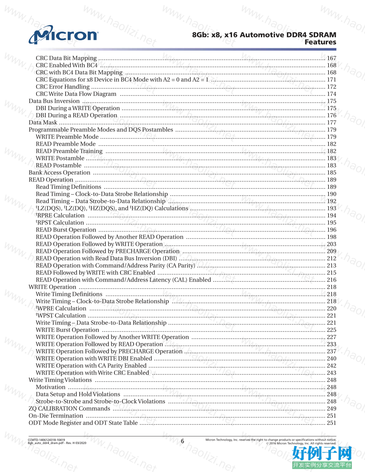
Contents
Important Notes and Warnings ....................................................................................................................... 18
General Notes and Description ....................................................................................................................... 18
Description ................................................................................................................................................ 18
Industrial Temperature ............................................................................................................................... 19
Automotive Temperature ............................................................................................................................ 19
Ultra-high Temperature .............................................................................................................................. 19
General Notes ............................................................................................................................................ 19
Definitions of the Device-Pin Signal Level ................................................................................................... 20
Definitions of the Bus Signal Level ............................................................................................................... 20
Functional Block Diagrams ............................................................................................................................. 21
Ball Assignments ............................................................................................................................................ 22
Ball Descriptions ............................................................................................................................................ 24
Package Dimensions ....................................................................................................................................... 27
State Diagram ................................................................................................................................................ 31
Functional Description ................................................................................................................................... 33
RESET and Initialization Procedure ................................................................................................................. 34
Power-Up and Initialization Sequence ......................................................................................................... 34
RESET Initialization with Stable Power Sequence ......................................................................................... 37
Uncontrolled Power-Down Sequence .......................................................................................................... 38
Programming Mode Registers ......................................................................................................................... 39
Mode Register 0 .............................................................................................................................................. 42
Burst Length, Type, and Order ..................................................................................................................... 43
CAS Latency ............................................................................................................................................... 44
Test Mode .................................................................................................................................................. 45
Write Recovery (WR)/READ-to-PRECHARGE ............................................................................................... 45
DLL RESET ................................................................................................................................................. 45
Mode Register 1 .............................................................................................................................................. 46
DLL Enable/DLL Disable ............................................................................................................................ 47
Output Driver Impedance Control ............................................................................................................... 48
ODT R TT(NOM) Values .................................................................................................................................. 48
Additive Latency ......................................................................................................................................... 48
Rx CTLE Control ......................................................................................................................................... 48
Write Leveling ............................................................................................................................................ 49
Output Disable ........................................................................................................................................... 49
Termination Data Strobe ............................................................................................................................. 49
Mode Register 2 .............................................................................................................................................. 50
CAS WRITE Latency .................................................................................................................................... 52
Low-Power Auto Self Refresh ....................................................................................................................... 52
Dynamic ODT ............................................................................................................................................ 52
Write Cyclic Redundancy Check Data Bus .................................................................................................... 52
Mode Register 3 .............................................................................................................................................. 53
Multipurpose Register ................................................................................................................................ 54
WRITE Command Latency When CRC/DM is Enabled ................................................................................. 55
Fine Granularity Refresh Mode .................................................................................................................... 55
Temperature Sensor Status ......................................................................................................................... 55
Per-DRAM Addressability ........................................................................................................................... 55
Gear-Down Mode ....................................................................................................................................... 55
Mode Register 4 .............................................................................................................................................. 56
Hard Post Package Repair Mode .................................................................................................................. 57
Soft Post Package Repair Mode .................................................................................................................... 57
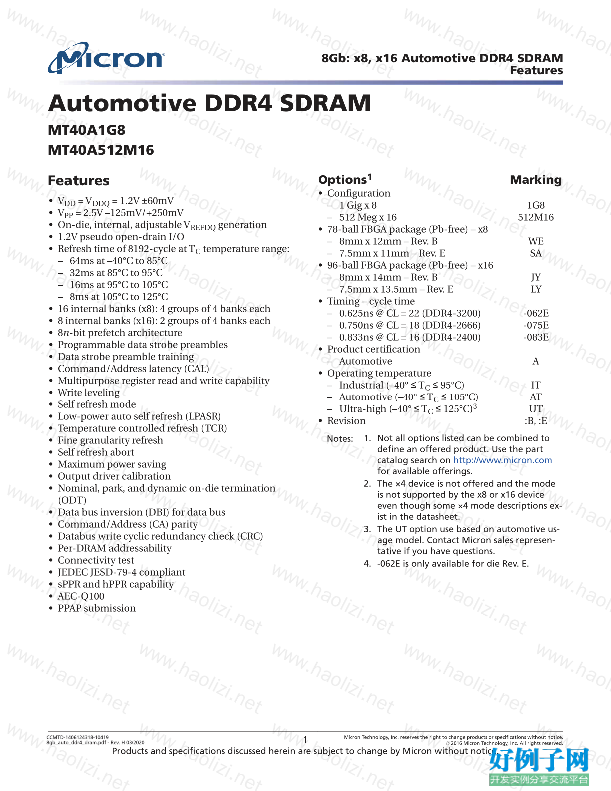
8Gb: x8, x16 Automotive DDR4 SDRAM
Features
CCMTD-1406124318-10419
8gb_auto_ddr4_dram.pdf - Rev. G 08/19 EN
3
Micron Technology, Inc. reserves the right to change products or specifications without notice.
? 2016 Micron Technology, Inc. All rights reserved.
WRITE Preamble ........................................................................................................................................ 58
READ Preamble .......................................................................................................................................... 58
READ Preamble Training ............................................................................................................................ 58
Temperature-Controlled Refresh ................................................................................................................. 58
Command Address Latency ........................................................................................................................ 58
Internal V REF Monitor ................................................................................................................................. 58
Maximum Power Savings Mode ................................................................................................................... 59
Mode Register 5 .............................................................................................................................................. 60
Data Bus Inversion ..................................................................................................................................... 61
Data Mask .................................................................................................................................................. 62
CA Parity Persistent Error Mode .................................................................................................................. 62
ODT Input Buffer for Power-Down .............................................................................................................. 62
CA Parity Error Status ................................................................................................................................. 62
CRC Error Status ......................................................................................................................................... 62
CA Parity Latency Mode .............................................................................................................................. 62
Mode Register 6 .............................................................................................................................................. 63
Data Rate Programming .............................................................................................................................. 64
V REFDQ Calibration Enable .......................................................................................................................... 64
V REFDQ Calibration Range ........................................................................................................................... 64
V REFDQ Calibration Value ............................................................................................................................ 64
Truth Tables ................................................................................................................................................... 65
NOP Command .............................................................................................................................................. 68
DESELECT Command .................................................................................................................................... 68
DLL-Off Mode ................................................................................................................................................ 68
DLL-On/Off Switching Procedures .................................................................................................................. 70
DLL Switch Sequence from DLL-On to DLL-Off ........................................................................................... 70
DLL-Off to DLL-On Procedure .................................................................................................................... 72
Input Clock Frequency Change ....................................................................................................................... 73
Write Leveling ................................................................................................................................................ 74
DRAM Setting for Write Leveling and DRAM TERMINATION Function in that Mode ..................................... 75
Procedure Description ................................................................................................................................ 76
Write Leveling Mode Exit ............................................................................................................................ 77
Command Address Latency ............................................................................................................................ 79
Low-Power Auto Self Refresh Mode ................................................................................................................. 84
Manual Self Refresh Mode .......................................................................................................................... 84
Multipurpose Register .................................................................................................................................... 86
MPR Reads ................................................................................................................................................. 87
MPR Readout Format ................................................................................................................................. 89
MPR Readout Serial Format ........................................................................................................................ 89
MPR Readout Parallel Format ..................................................................................................................... 90
MPR Readout Staggered Format .................................................................................................................. 91
MPR READ Waveforms ............................................................................................................................... 92
MPR Writes ................................................................................................................................................ 94
MPR WRITE Waveforms .............................................................................................................................. 95
MPR REFRESH Waveforms ......................................................................................................................... 96
Gear-Down Mode ........................................................................................................................................... 99
Maximum Power-Saving Mode ....................................................................................................................... 102
Maximum Power-Saving Mode Entry .......................................................................................................... 102
Maximum Power-Saving Mode Entry in PDA .............................................................................................. 103
CKE Transition During Maximum Power-Saving Mode ................................................................................ 103
Maximum Power-Saving Mode Exit ............................................................................................................ 103
Command/Address Parity .............................................................................................................................. 105
8Gb: x8, x16 Automotive DDR4 SDRAM
Features
CCMTD-1406124318-10419
8gb_auto_ddr4_dram.pdf - Rev. G 08/19 EN
4
Micron Technology, Inc. reserves the right to change products or specifications without notice.
? 2016 Micron Technology, Inc. All rights reserved.
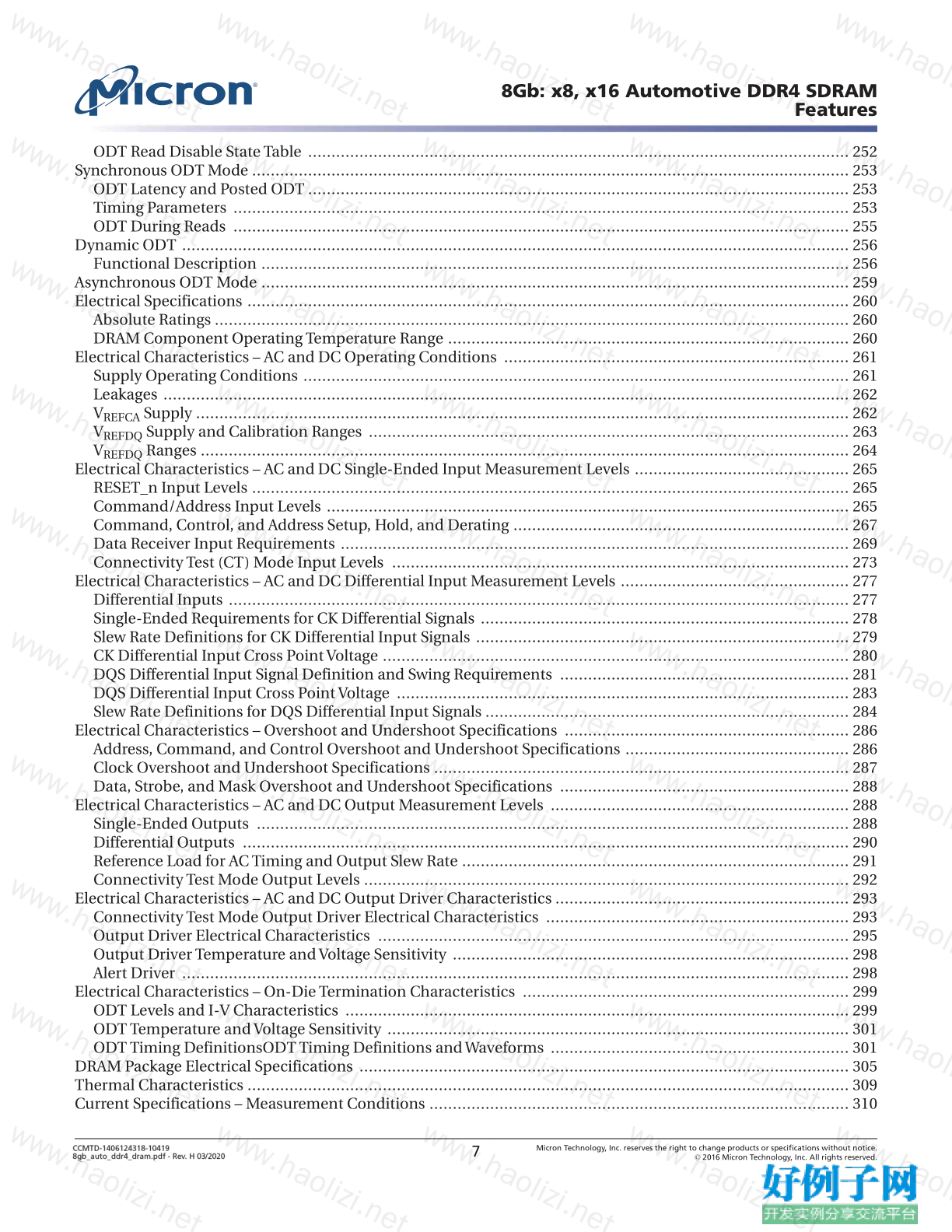
Per-DRAM Addressability .............................................................................................................................. 113
V REFDQ Calibration ........................................................................................................................................ 116
V REFDQ Range and Levels ........................................................................................................................... 117
V REFDQ Step Size ........................................................................................................................................ 117
V REFDQ Increment and Decrement Timing .................................................................................................. 118
V REFDQ Target Settings ............................................................................................................................... 122
Connectivity Test Mode ................................................................................................................................. 124
Pin Mapping ............................................................................................................................................. 124
Minimum Terms Definition for Logic Equations ......................................................................................... 125
Logic Equations for a ×4 Device .................................................................................................................. 125
Logic Equations for a ×8 Device .................................................................................................................. 126
Logic Equations for a ×16 Device ................................................................................................................ 126
CT Input Timing Requirements .................................................................................................................. 126
Excessive Row Activation ............................................................................................................................... 128
Post Package Repair ....................................................................................................................................... 129
Post Package Repair ................................................................................................................................... 129
Hard Post Package Repair .............................................................................................................................. 130
hPPR Row Repair - Entry ............................................................................................................................ 130
hPPR Row Repair – WRA Initiated (REF Commands Allowed) ...................................................................... 130
hPPR Row Repair – WR Initiated (REF Commands NOT Allowed) ................................................................. 132
sPPR Row Repair ........................................................................................................................................... 134
hPPR/sPPR Support Identifier ........................................................................................................................ 137
ACTIVATE Command .................................................................................................................................... 137
PRECHARGE Command ................................................................................................................................ 138
REFRESH Command ..................................................................................................................................... 138
Temperature-Controlled Refresh Mode .......................................................................................................... 141
Normal Temperature Mode ........................................................................................................................ 141
Extended Temperature Mode ..................................................................................................................... 141
Fine Granularity Refresh Mode ....................................................................................................................... 144
Mode Register and Command Truth Table .................................................................................................. 144
t REFI and t RFC Parameters ........................................................................................................................ 144
Changing Refresh Rate ............................................................................................................................... 147
Usage with TCR Mode ................................................................................................................................ 147
Self Refresh Entry and Exit ......................................................................................................................... 147
SELF REFRESH Operation .............................................................................................................................. 149
Self Refresh Abort ...................................................................................................................................... 151
Self Refresh Exit with NOP Command ......................................................................................................... 152
Power-Down Mode ........................................................................................................................................ 154
Power-Down Clarifications – Case 1 ........................................................................................................... 159
Power-Down Entry, Exit Timing with CAL ................................................................................................... 160
ODT Input Buffer Disable Mode for Power-Down ............................................................................................ 162
CRC Write Data Feature ................................................................................................................................. 164
CRC Write Data ......................................................................................................................................... 164
WRITE CRC DATA Operation ...................................................................................................................... 164
DBI_n and CRC Both Enabled .................................................................................................................... 165
DM_n and CRC Both Enabled .................................................................................................................... 165
DM_n and DBI_n Conflict During Writes with CRC Enabled ........................................................................ 165
CRC and Write Preamble Restrictions ......................................................................................................... 165
CRC Simultaneous Operation Restrictions .................................................................................................. 165
CRC Polynomial ........................................................................................................................................ 165
CRC Combinatorial Logic Equations .......................................................................................................... 166
Burst Ordering for BL8 ............................................................................................................................... 167
8Gb: x8, x16 Automotive DDR4 SDRAM
Features
CCMTD-1406124318-10419
8gb_auto_ddr4_dram.pdf - Rev. G 08/19 EN
5
Micron Technology, Inc. reserves the right to change products or specifications without notice.
? 2016 Micron Technology, Inc. All rights reserved.
CRC Data Bit Mapping ............................................................................................................................... 167
CRC Enabled With BC4 .............................................................................................................................. 168
CRC with BC4 Data Bit Mapping ................................................................................................................ 168
CRC Equations for x8 Device in BC4 Mode with A2 = 0 and A2 = 1 ................................................................ 171
CRC Error Handling ................................................................................................................................... 172
CRC Write Data Flow Diagram ................................................................................................................... 174
Data Bus Inversion ........................................................................................................................................ 175
DBI During a WRITE Operation .................................................................................................................. 175
DBI During a READ Operation ................................................................................................................... 176
Data Mask ..................................................................................................................................................... 177
Programmable Preamble Modes and DQS Postambles .................................................................................... 179
WRITE Preamble Mode .............................................................................................................................. 179
READ Preamble Mode ............................................................................................................................... 182
READ Preamble Training ........................................................................................................................... 182
WRITE Postamble ...................................................................................................................................... 183
READ Postamble ....................................................................................................................................... 183
Bank Access Operation .................................................................................................................................. 185
READ Operation ............................................................................................................................................ 189
Read Timing Definitions ............................................................................................................................ 189
Read Timing – Clock-to-Data Strobe Relationship ....................................................................................... 190
Read Timing – Data Strobe-to-Data Relationship ........................................................................................ 192
t LZ(DQS), t LZ(DQ), t HZ(DQS), and t HZ(DQ) Calculations ............................................................................ 193
t RPRE Calculation ..................................................................................................................................... 194
t RPST Calculation ...................................................................................................................................... 195
READ Burst Operation ............................................................................................................................... 196
READ Operation Followed by Another READ Operation .............................................................................. 198
READ Operation Followed by WRITE Operation .......................................................................................... 203
READ Operation Followed by PRECHARGE Operation ................................................................................ 209
READ Operation with Read Data Bus Inversion (DBI) .................................................................................. 212
READ Operation with Command/Address Parity (CA Parity) ........................................................................ 213
READ Followed by WRITE with CRC Enabled .............................................................................................. 215
READ Operation with Command/Address Latency (CAL) Enabled ............................................................... 216
WRITE Operation .......................................................................................................................................... 218
Write Timing Definitions ........................................................................................................................... 218
Write Timing – Clock-to-Data Strobe Relationship ...................................................................................... 218
t WPRE Calculation .................................................................................................................................... 220
t WPST Calculation ..................................................................................................................................... 221
Write Timing – Data Strobe-to-Data Relationship ........................................................................................ 221
WRITE Burst Operation ............................................................................................................................. 225
WRITE Operation Followed by Another WRITE Operation ........................................................................... 227
WRITE Operation Followed by READ Operation .......................................................................................... 233
WRITE Operation Followed by PRECHARGE Operation ............................................................................... 237
WRITE Operation with WRITE DBI Enabled ................................................................................................ 240
WRITE Operation with CA Parity Enabled ................................................................................................... 242
WRITE Operation with Write CRC Enabled ................................................................................................. 243
Write Timing Violations ................................................................................................................................. 248
Motivation ................................................................................................................................................ 248
Data Setup and Hold Violations ................................................................................................................. 248
Strobe-to-Strobe and Strobe-to-Clock Violations ........................................................................................ 248
ZQ CALIBRATION Commands ....................................................................................................................... 249
On-Die Termination ...................................................................................................................................... 251
ODT Mode Register and ODT State Table ........................................................................................................ 251
8Gb: x8, x16 Automotive DDR4 SDRAM
Features
CCMTD-1406124318-10419
8gb_auto_ddr4_dram.pdf - Rev. G 08/19 EN
6
Micron Technology, Inc. reserves the right to change products or specifications without notice.
? 2016 Micron Technology, Inc. All rights reserved.
ODT Read Disable State Table .................................................................................................................... 252
Synchronous ODT Mode ................................................................................................................................ 253
ODT Latency and Posted ODT .................................................................................................................... 253
Timing Parameters .................................................................................................................................... 253
ODT During Reads .................................................................................................................................... 255
Dynamic ODT ............................................................................................................................................... 256
Functional Description .............................................................................................................................. 256
Asynchronous ODT Mode .............................................................................................................................. 259
Electrical Specifications ................................................................................................................................. 260
Absolute Ratings ........................................................................................................................................ 260
DRAM Component Operating Temperature Range ...................................................................................... 260
Electrical Characteristics – AC and DC Operating Conditions .......................................................................... 261
Supply Operating Conditions ..................................................................................................................... 261
Leakages ................................................................................................................................................... 262
V REFCA Supply ............................................................................................................................................ 262
V REFDQ Supply and Calibration Ranges ....................................................................................................... 263
V REFDQ Ranges ........................................................................................................................................... 264
Electrical Characteristics – AC and DC Single-Ended Input Measurement Levels .............................................. 265
RESET_n Input Levels ................................................................................................................................ 265
Command/Address Input Levels ................................................................................................................ 265
Command, Control, and Address Setup, Hold, and Derating ........................................................................ 267
Data Receiver Input Requirements ............................................................................................................. 269
Connectivity Test (CT) Mode Input Levels .................................................................................................. 273
Electrical Characteristics – AC and DC Differential Input Measurement Levels ................................................. 277
Differential Inputs ..................................................................................................................................... 277
Single-Ended Requirements for CK Differential Signals ............................................................................... 278
Slew Rate Definitions for CK Differential Input Signals ................................................................................ 279
CK Differential Input Cross Point Voltage .................................................................................................... 280
DQS Differential Input Signal Definition and Swing Requirements .............................................................. 281
DQS Differential Input Cross Point Voltage ................................................................................................. 283
Slew Rate Definitions for DQS Differential Input Signals .............................................................................. 284
Electrical Characteristics – Overshoot and Undershoot Specifications ............................................................. 286
Address, Command, and Control Overshoot and Undershoot Specifications ................................................ 286
Clock Overshoot and Undershoot Specifications ......................................................................................... 287
Data, Strobe, and Mask Overshoot and Undershoot Specifications .............................................................. 288
Electrical Characteristics – AC and DC Output Measurement Levels ................................................................ 288
Single-Ended Outputs ............................................................................................................................... 288
Differential Outputs .................................................................................................................................. 290
Reference Load for AC Timing and Output Slew Rate ................................................................................... 291
Connectivity Test Mode Output Levels ........................................................................................................ 292
Electrical Characteristics – AC and DC Output Driver Characteristics ............................................................... 293
Connectivity Test Mode Output Driver Electrical Characteristics ................................................................. 293
Output Driver Electrical Characteristics ..................................................................................................... 295
Output Driver Temperature and Voltage Sensitivity ..................................................................................... 298
Alert Driver ............................................................................................................................................... 298
Electrical Characteristics – On-Die Termination Characteristics ...................................................................... 299
ODT Levels and I-V Characteristics ............................................................................................................ 299
ODT Temperature and Voltage Sensitivity ................................................................................................... 301
ODT Timing DefinitionsODT Timing Definitions and Waveforms ................................................................ 301
DRAM Package Electrical Specifications ......................................................................................................... 305
Thermal Characteristics ................................................................................................................................. 309
Current Specifications – Measurement Conditions .......................................................................................... 310
8Gb: x8, x16 Automotive DDR4 SDRAM
Features
CCMTD-1406124318-10419
8gb_auto_ddr4_dram.pdf - Rev. G 08/19 EN
7
Micron Technology, Inc. reserves the right to change products or specifications without notice.
? 2016 Micron Technology, Inc. All rights reserved.
I DD , I PP , and I DDQ Measurement Conditions ................................................................................................ 310
I DD Definitions .......................................................................................................................................... 312
Current Specifications – Patterns and Test Conditions ..................................................................................... 316
Current Test Definitions and Patterns ......................................................................................................... 316
I DD Specifications ...................................................................................................................................... 325
Current Specifications – Limits ....................................................................................................................... 326
Speed Bin Tables ........................................................................................................................................... 337
Backward Compatibility ............................................................................................................................ 337
.................................................................................................................................................................. 339
.................................................................................................................................................................. 341
.................................................................................................................................................................. 343
.................................................................................................................................................................. 345
.................................................................................................................................................................. 347
.................................................................................................................................................................. 350
.................................................................................................................................................................. 353
Refresh Parameters By Device Density ............................................................................................................ 356
Electrical Characteristics and AC Timing Parameters ...................................................................................... 357
Electrical Characteristics and AC Timing Parameters: 2666 Through 3200 ........................................................ 369
Converting Time-Based Specifications to Clock-Based Requirements .............................................................. 380
Options Tables .............................................................................................................................................. 382
8Gb: x8, x16 Automotive DDR4 SDRAM
Features
CCMTD-1406124318-10419
8gb_auto_ddr4_dram.pdf - Rev. G 08/19 EN
8
Micron Technology, Inc. reserves the right to change products or specifications without notice.
? 2016 Micron Technology, Inc. All rights reserved.
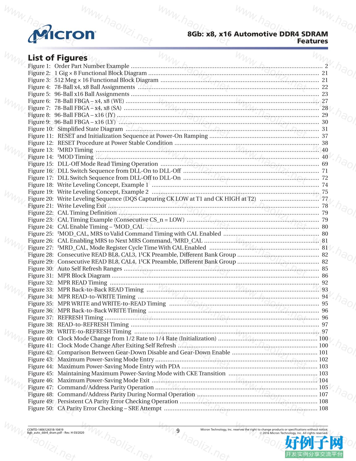
List of Figures
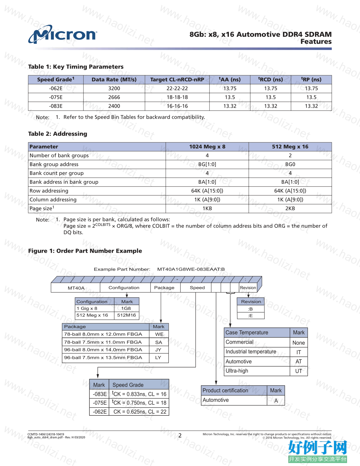
Figure 1: Order Part Number Example .............................................................................................................. 2
Figure 2: 1 Gig × 8 Functional Block Diagram .................................................................................................. 21
Figure 3: 512 Meg × 16 Functional Block Diagram ........................................................................................... 21
Figure 4: 78-Ball x4, x8 Ball Assignments ........................................................................................................ 22
Figure 5: 96-Ball x16 Ball Assignments ............................................................................................................ 23
Figure 6: 78-Ball FBGA – x4, x8 (WE) ............................................................................................................... 27
Figure 7: 78-Ball FBGA – x4, x8 (SA) ................................................................................................................ 28
Figure 8: 96-Ball FBGA – x16 (JY) .................................................................................................................... 29
Figure 9: 96-Ball FBGA – x16 (LY) ................................................................................................................... 30
Figure 10: Simplified State Diagram ............................................................................................................... 31
Figure 11: RESET and Initialization Sequence at Power-On Ramping ............................................................... 37
Figure 12: RESET Procedure at Power Stable Condition ................................................................................... 38
Figure 13: t MRD Timing ................................................................................................................................ 40
Figure 14: t MOD Timing ................................................................................................................................ 40
Figure 15: DLL-Off Mode Read Timing Operation ........................................................................................... 69
Figure 16: DLL Switch Sequence from DLL-On to DLL-Off .............................................................................. 71
Figure 17: DLL Switch Sequence from DLL-Off to DLL-On .............................................................................. 72
Figure 18: Write Leveling Concept, Example 1 ................................................................................................ 74
Figure 19: Write Leveling Concept, Example 2 ................................................................................................ 75
Figure 20: Write Leveling Sequence (DQS Capturing CK LOW at T1 and CK HIGH at T2) .................................. 77
Figure 21: Write Leveling Exit ......................................................................................................................... 78
Figure 22: CAL Timing Definition ................................................................................................................... 79
Figure 23: CAL Timing Example (Consecutive CS_n = LOW) ............................................................................ 79
Figure 24: CAL Enable Timing – t MOD_CAL ................................................................................................... 80
Figure 25: t MOD_CAL, MRS to Valid Command Timing with CAL Enabled ....................................................... 80
Figure 26: CAL Enabling MRS to Next MRS Command, t MRD_CAL .................................................................. 81
Figure 27: t MRD_CAL, Mode Register Cycle Time With CAL Enabled ............................................................... 81
Figure 28: Consecutive READ BL8, CAL3, 1 t CK Preamble, Different Bank Group ............................................... 82
Figure 29: Consecutive READ BL8, CAL4, 1 t CK Preamble, Different Bank Group ............................................... 82
Figure 30: Auto Self Refresh Ranges ................................................................................................................ 85
Figure 31: MPR Block Diagram ....................................................................................................................... 86
Figure 32: MPR READ Timing ........................................................................................................................ 92
Figure 33: MPR Back-to-Back READ Timing ................................................................................................... 93
Figure 34: MPR READ-to-WRITE Timing ........................................................................................................ 94
Figure 35: MPR WRITE and WRITE-to-READ Timing ...................................................................................... 95
Figure 36: MPR Back-to-Back WRITE Timing .................................................................................................. 96
Figure 37: REFRESH Timing ........................................................................................................................... 96
Figure 38: READ-to-REFRESH Timing ............................................................................................................ 97
Figure 39: WRITE-to-REFRESH Timing .......................................................................................................... 97
Figure 40: Clock Mode Change from 1/2 Rate to 1/4 Rate (Initialization) ......................................................... 100
Figure 41: Clock Mode Change After Exiting Self Refresh ................................................................................ 100
Figure 42: Comparison Between Gear-Down Disable and Gear-Down Enable ................................................. 101
Figure 43: Maximum Power-Saving Mode Entry ............................................................................................. 102
Figure 44: Maximum Power-Saving Mode Entry with PDA .............................................................................. 103
Figure 45: Maintaining Maximum Power-Saving Mode with CKE Transition ................................................... 103
Figure 46: Maximum Power-Saving Mode Exit ............................................................................................... 104
Figure 47: Command/Address Parity Operation ............................................................................................. 105
Figure 48: Command/Address Parity During Normal Operation ..................................................................... 107
Figure 49: Persistent CA Parity Error Checking Operation ............................................................................... 108
Figure 50: CA Parity Error Checking – SRE Attempt ........................................................................................ 108
8Gb: x8, x16 Automotive DDR4 SDRAM
Features
CCMTD-1406124318-10419
8gb_auto_ddr4_dram.pdf - Rev. G 08/19 EN
9
Micron Technology, Inc. reserves the right to change products or specifications without notice.
? 2016 Micron Technology, Inc. All rights reserved.
Figure 51: CA Parity Error Checking – SRX Attempt ........................................................................................ 109
Figure 52: CA Parity Error Checking – PDE/PDX ............................................................................................ 109
Figure 53: Parity Entry Timing Example – t MRD_PAR ..................................................................................... 110
Figure 54: Parity Entry Timing Example – t MOD_PAR ..................................................................................... 110
Figure 55: Parity Exit Timing Example – t MRD_PAR ....................................................................................... 110
Figure 56: Parity Exit Timing Example – t MOD_PAR ....................................................................................... 111
Figure 57: CA Parity Flow Diagram ................................................................................................................ 112
Figure 58: PDA Operation Enabled, BL8 ........................................................................................................ 114
Figure 59: PDA Operation Enabled, BC4 ........................................................................................................ 114
Figure 60: MRS PDA Exit ............................................................................................................................... 115
Figure 61: V REFDQ Voltage Range ................................................................................................................... 116
Figure 62: Example of V REF Set Tolerance and Step Size .................................................................................. 118
Figure 63: V REFDQ Timing Diagram for V REF,time Parameter .............................................................................. 119
Figure 64: V REFDQ Training Mode Entry and Exit Timing Diagram ................................................................... 120
Figure 65: V REF Step: Single Step Size Increment Case .................................................................................... 121
Figure 66: V REF Step: Single Step Size Decrement Case ................................................................................... 121
Figure 67: V REF Full Step: From V REF,min to V REF,max Case .................................................................................. 122
Figure 68: V REF Full Step: From V REF,max to V REF,min Case .................................................................................. 122
Figure 69: V REFDQ Equivalent Circuit ............................................................................................................. 123
Figure 70: Connectivity Test Mode Entry ....................................................................................................... 127
Figure 71: hPPR WRA – Entry ........................................................................................................................ 132
Figure 72: hPPR WRA – Repair and Exit ......................................................................................................... 132
Figure 73: hPPR WR – Entry .......................................................................................................................... 133
Figure 74: hPPR WR – Repair and Exit ............................................................................................................ 133
Figure 75: sPPR – Entry ................................................................................................................................. 136
Figure 76: sPPR – Repair, and Exit ................................................................................................................. 136
Figure 77: t RRD Timing ................................................................................................................................ 137
Figure 78: t FAW Timing ................................................................................................................................. 138
Figure 79: REFRESH Command Timing ......................................................................................................... 139
Figure 80: Postponing REFRESH Commands (Example) ................................................................................. 140
Figure 81: Pulling In REFRESH Commands (Example) ................................................................................... 140
Figure 82: TCR Mode Example 1 ..................................................................................................................... 143
Figure 83: 4Gb with Fine Granularity Refresh Mode Example ......................................................................... 146
Figure 84: OTF REFRESH Command Timing ................................................................................................. 147
Figure 85: Self Refresh Entry/Exit Timing ...................................................................................................... 150
Figure 86: Self Refresh Entry/Exit Timing with CAL Mode ............................................................................... 151
Figure 87: Self Refresh Abort ......................................................................................................................... 152
Figure 88: Self Refresh Exit with NOP Command ............................................................................................ 153
Figure 89: Active Power-Down Entry and Exit ................................................................................................ 155
Figure 90: Power-Down Entry After Read and Read with Auto Precharge ......................................................... 156
Figure 91: Power-Down Entry After Write and Write with Auto Precharge ........................................................ 156
Figure 92: Power-Down Entry After Write ...................................................................................................... 157
Figure 93: Precharge Power-Down Entry and Exit .......................................................................................... 157
Figure 94: REFRESH Command to Power-Down Entry ................................................................................... 158
Figure 95: Active Command to Power-Down Entry ......................................................................................... 158
Figure 96: PRECHARGE/PRECHARGE ALL Command to Power-Down Entry .................................................. 159
Figure 97: MRS Command to Power-Down Entry ........................................................................................... 159
Figure 98: Power-Down Entry/Exit Clarifications – Case 1 .............................................................................. 160
Figure 99: Active Power-Down Entry and Exit Timing with CAL ...................................................................... 160
Figure 100: REFRESH Command to Power-Down Entry with CAL ................................................................... 161
Figure 101: ODT Power-Down Entry with ODT Buffer Disable Mode .............................................................. 162
Figure 102: ODT Power-Down Exit with ODT Buffer Disable Mode ................................................................. 163
8Gb: x8, x16 Automotive DDR4 SDRAM
Features
CCMTD-1406124318-10419
8gb_auto_ddr4_dram.pdf - Rev. G 08/19 EN
10
Micron Technology, Inc. reserves the right to change products or specifications without notice.
? 2016 Micron Technology, Inc. All rights reserved.
Figure 103: CRC Write Data Operation .......................................................................................................... 164
Figure 104: CRC Error Reporting ................................................................................................................... 173
Figure 105: CA Parity Flow Diagram .............................................................................................................. 174
Figure 106: 1 t CK vs. 2 t CK WRITE Preamble Mode ........................................................................................... 179
Figure 107: 1 t CK vs. 2 t CK WRITE Preamble Mode, t CCD = 4 ............................................................................ 180
Figure 108: 1 t CK vs. 2 t CK WRITE Preamble Mode, t CCD = 5 ............................................................................ 181
Figure 109: 1 t CK vs. 2 t CK WRITE Preamble Mode, t CCD = 6 ........................................................................... 181
Figure 110: 1 t CK vs. 2 t CK READ Preamble Mode ............................................................................................ 182
Figure 111: READ Preamble Training ............................................................................................................. 183
Figure 112: WRITE Postamble ....................................................................................................................... 183
Figure 113: READ Postamble ........................................................................................................................ 184
Figure 114: Bank Group x4/x8 Block Diagram ................................................................................................ 185
Figure 115: READ Burst t CCD_S and t CCD_L Examples .................................................................................. 186
Figure 116: Write Burst t CCD_S and t CCD_L Examples ................................................................................... 186
Figure 117: t RRD Timing ............................................................................................................................... 187
Figure 118: t WTR_S Timing (WRITE-to-READ, Different Bank Group, CRC and DM Disabled) ......................... 187
Figure 119: t WTR_L Timing (WRITE-to-READ, Same Bank Group, CRC and DM Disabled) .............................. 188
Figure 120: Read Timing Definition ............................................................................................................... 190
Figure 121: Clock-to-Data Strobe Relationship .............................................................................................. 191
Figure 122: Data Strobe-to-Data Relationship ................................................................................................ 192
Figure 123: t LZ and t HZ Method for Calculating Transitions and Endpoints .................................................... 193
Figure 124: t RPRE Method for Calculating Transitions and Endpoints ............................................................. 194
Figure 125: t RPST Method for Calculating Transitions and Endpoints ............................................................. 195
Figure 126: READ Burst Operation, RL = 11 (AL = 0, CL = 11, BL8) ................................................................... 196
Figure 127: READ Burst Operation, RL = 21 (AL = 10, CL = 11, BL8) ................................................................. 197
Figure 128: Consecutive READ (BL8) with 1 t CK Preamble in Different Bank Group .......................................... 198
Figure 129: Consecutive READ (BL8) with 2 t CK Preamble in Different Bank Group .......................................... 198
Figure 130: Nonconsecutive READ (BL8) with 1 t CK Preamble in Same or Different Bank Group ....................... 199
Figure 131: Nonconsecutive READ (BL8) with 2 t CK Preamble in Same or Different Bank Group ....................... 199
Figure 132: READ (BC4) to READ (BC4) with 1 t CK Preamble in Different Bank Group ...................................... 200
Figure 133: READ (BC4) to READ (BC4) with 2 t CK Preamble in Different Bank Group ...................................... 200
Figure 134: READ (BL8) to READ (BC4) OTF with 1 t CK Preamble in Different Bank Group ............................... 201
Figure 135: READ (BL8) to READ (BC4) OTF with 2 t CK Preamble in Different Bank Group ............................... 201
Figure 136: READ (BC4) to READ (BL8) OTF with 1 t CK Preamble in Different Bank Group ............................... 202
Figure 137: READ (BC4) to READ (BL8) OTF with 2 t CK Preamble in Different Bank Group ............................... 202
Figure 138: READ (BL8) to WRITE (BL8) with 1 t CK Preamble in Same or Different Bank Group ........................ 203
Figure 139: READ (BL8) to WRITE (BL8) with 2 t CK Preamble in Same or Different Bank Group ........................ 203
Figure 140: READ (BC4) OTF to WRITE (BC4) OTF with 1 t CK Preamble in Same or Different Bank Group ......... 204
Figure 141: READ (BC4) OTF to WRITE (BC4) OTF with 2 t CK Preamble in Same or Different Bank Group ......... 205
Figure 142: READ (BC4) Fixed to WRITE (BC4) Fixed with 1 t CK Preamble in Same or Different Bank Group ..... 205
Figure 143: READ (BC4) Fixed to WRITE (BC4) Fixed with 2 t CK Preamble in Same or Different Bank Group ..... 206
Figure 144: READ (BC4) to WRITE (BL8) OTF with 1 t CK Preamble in Same or Different Bank Group ................ 207
Figure 145: READ (BC4) to WRITE (BL8) OTF with 2 t CK Preamble in Same or Different Bank Group ................ 207
Figure 146: READ (BL8) to WRITE (BC4) OTF with 1 t CK Preamble in Same or Different Bank Group ................ 208
Figure 147: READ (BL8) to WRITE (BC4) OTF with 2 t CK Preamble in Same or Different Bank Group ................ 208
Figure 148: READ to PRECHARGE with 1 t CK Preamble .................................................................................. 209
Figure 149: READ to PRECHARGE with 2 t CK Preamble .................................................................................. 210
Figure 150: READ to PRECHARGE with Additive Latency and 1 t CK Preamble .................................................. 210
Figure 151: READ with Auto Precharge and 1 t CK Preamble ............................................................................ 211
Figure 152: READ with Auto Precharge, Additive Latency, and 1 t CK Preamble ................................................. 212
Figure 153: Consecutive READ (BL8) with 1 t CK Preamble and DBI in Different Bank Group ............................ 212
Figure 154: Consecutive READ (BL8) with 1 t CK Preamble and CA Parity in Different Bank Group .................... 213
8Gb: x8, x16 Automotive DDR4 SDRAM
Features
CCMTD-1406124318-10419
8gb_auto_ddr4_dram.pdf - Rev. G 08/19 EN
11
Micron Technology, Inc. reserves the right to change products or specifications without notice.
? 2016 Micron Technology, Inc. All rights reserved.
Figure 155: READ (BL8) to WRITE (BL8) with 1 t CK Preamble and CA Parity in Same or Different Bank Group ... 214
Figure 156: READ (BL8) to WRITE (BL8 or BC4: OTF) with 1 t CK Preamble and Write CRC in Same or Different
Bank Group ............................................................................................................................................... 215
Figure 157: READ (BC4: Fixed) to WRITE (BC4: Fixed) with 1 t CK Preamble and Write CRC in Same or Different
Bank Group ............................................................................................................................................... 216
Figure 158: Consecutive READ (BL8) with CAL (3 t CK) and 1 t CK Preamble in Different Bank Group .................. 216
Figure 159: Consecutive READ (BL8) with CAL (4 t CK) and 1 t CK Preamble in Different Bank Group .................. 217
Figure 160: Write Timing Definition .............................................................................................................. 219
Figure 161: t WPRE Method for Calculating Transitions and Endpoints ............................................................ 220
Figure 162: t WPST Method for Calculating Transitions and Endpoints ............................................................ 221
Figure 163: Rx Compliance Mask .................................................................................................................. 222
Figure 164: V CENT_DQ V REFDQ Voltage Variation .............................................................................................. 222
Figure 165: Rx Mask DQ-to-DQS Timings ...................................................................................................... 223
Figure 166: Rx Mask DQ-to-DQS DRAM-Based Timings ................................................................................. 224
Figure 167: Example of Data Input Requirements Without Training ................................................................ 225
Figure 168: WRITE Burst Operation, WL = 9 (AL = 0, CWL = 9, BL8) ................................................................. 226
Figure 169: WRITE Burst Operation, WL = 19 (AL = 10, CWL = 9, BL8) ............................................................. 227
Figure 170: Consecutive WRITE (BL8) with 1 t CK Preamble in Different Bank Group ........................................ 227
Figure 171: Consecutive WRITE (BL8) with 2 t CK Preamble in Different Bank Group ........................................ 228
Figure 172: Nonconsecutive WRITE (BL8) with 1 t CK Preamble in Same or Different Bank Group ..................... 229
Figure 173: Nonconsecutive WRITE (BL8) with 2 t CK Preamble in Same or Different Bank Group ..................... 229
Figure 174: WRITE (BC4) OTF to WRITE (BC4) OTF with 1 t CK Preamble in Different Bank Group .................... 230
Figure 175: WRITE (BC4) OTF to WRITE (BC4) OTF with 2 t CK Preamble in Different Bank Group .................... 231
Figure 176: WRITE (BC4) Fixed to WRITE (BC4) Fixed with 1 t CK Preamble in Different Bank Group ................. 231
Figure 177: WRITE (BL8) to WRITE (BC4) OTF with 1 t CK Preamble in Different Bank Group ............................ 232
Figure 178: WRITE (BC4) OTF to WRITE (BL8) with 1 t CK Preamble in Different Bank Group ............................ 233
Figure 179: WRITE (BL8) to READ (BL8) with 1 t CK Preamble in Different Bank Group ..................................... 233
Figure 180: WRITE (BL8) to READ (BL8) with 1 t CK Preamble in Same Bank Group .......................................... 234
Figure 181: WRITE (BC4) OTF to READ (BC4) OTF with 1 t CK Preamble in Different Bank Group ...................... 235
Figure 182: WRITE (BC4) OTF to READ (BC4) OTF with 1 t CK Preamble in Same Bank Group ........................... 235
Figure 183: WRITE (BC4) Fixed to READ (BC4) Fixed with 1 t CK Preamble in Different Bank Group ................. 236
Figure 184: WRITE (BC4) Fixed to READ (BC4) Fixed with 1 t CK Preamble in Same Bank Group ....................... 236
Figure 185: WRITE (BL8/BC4-OTF) to PRECHARGE with 1 t CK Preamble ........................................................ 237
Figure 186: WRITE (BC4-Fixed) to PRECHARGE with 1 t CK Preamble .............................................................. 238
Figure 187: WRITE (BL8/BC4-OTF) to Auto PRECHARGE with 1 t CK Preamble ................................................ 238
Figure 188: WRITE (BC4-Fixed) to Auto PRECHARGE with 1 t CK Preamble ...................................................... 239
Figure 189: WRITE (BL8/BC4-OTF) with 1 t CK Preamble and DBI ................................................................... 240
Figure 190: WRITE (BC4-Fixed) with 1 t CK Preamble and DBI ......................................................................... 241
Figure 191: Consecutive Write (BL8) with 1 t CK Preamble and CA Parity in Different Bank Group ..................... 242
Figure 192: Consecutive WRITE (BL8/BC4-OTF) with 1 t CK Preamble and Write CRC in Same or Different Bank
Group ....................................................................................................................................................... 243
Figure 193: Consecutive WRITE (BC4-Fixed) with 1 t CK Preamble and Write CRC in Same or Different Bank
Group ....................................................................................................................................................... 244
Figure 194: Nonconsecutive WRITE (BL8/BC4-OTF) with 1 t CK Preamble and Write CRC in Same or Different
Bank Group ............................................................................................................................................... 245
Figure 195: Nonconsecutive WRITE (BL8/BC4-OTF) with 2 t CK Preamble and Write CRC in Same or Different
Bank Group ............................................................................................................................................... 246
Figure 196: WRITE (BL8/BC4-OTF/Fixed) with 1 t CK Preamble and Write CRC in Same or Different Bank Group ... 247
Figure 197: ZQ Calibration Timing ................................................................................................................ 250
Figure 198: Functional Representation of ODT .............................................................................................. 251
Figure 199: Synchronous ODT Timing with BL8 ............................................................................................. 254
Figure 200: Synchronous ODT with BC4 ........................................................................................................ 254
8Gb: x8, x16 Automotive DDR4 SDRAM
Features
CCMTD-1406124318-10419
8gb_auto_ddr4_dram.pdf - Rev. G 08/19 EN
12
Micron Technology, Inc. reserves the right to change products or specifications without notice.
? 2016 Micron Technology, Inc. All rights reserved.
Figure 201: ODT During Reads ...................................................................................................................... 255
Figure 202: Dynamic ODT (1 t CK Preamble; CL = 14, CWL = 11, BL = 8, AL = 0, CRC Disabled) .......................... 257
Figure 203: Dynamic ODT Overlapped with R TT(NOM) (CL = 14, CWL = 11, BL = 8, AL = 0, CRC Disabled) .......... 258
Figure 204: Asynchronous ODT Timings with DLL Off ................................................................................... 259
Figure 205: V REFDQ Voltage Range .................................................................................................................. 262
Figure 206: RESET_n Input Slew Rate Definition ............................................................................................ 265
Figure 207: Single-Ended Input Slew Rate Definition ..................................................................................... 267
Figure 208: DQ Slew Rate Definitions ............................................................................................................ 270
Figure 209: Rx Mask Relative to t DS/ t DH ....................................................................................................... 272
Figure 210: Rx Mask Without Write Training .................................................................................................. 273
Figure 211: TEN Input Slew Rate Definition ................................................................................................... 274
Figure 212: CT Type-A Input Slew Rate Definition .......................................................................................... 274
Figure 213: CT Type-B Input Slew Rate Definition .......................................................................................... 275
Figure 214: CT Type-C Input Slew Rate Definition .......................................................................................... 276
Figure 215: CT Type-D Input Slew Rate Definition ......................................................................................... 276
Figure 216: Differential AC Swing and “Time Exceeding AC-Level” t DVAC ....................................................... 277
Figure 217: Single-Ended Requirements for CK .............................................................................................. 279
Figure 218: Differential Input Slew Rate Definition for CK_t, CK_c .................................................................. 280
Figure 219: V IX(CK) Definition ........................................................................................................................ 280
Figure 220: Differential Input Signal Definition for DQS_t, DQS_c .................................................................. 281
Figure 221: DQS_t, DQS_c Input Peak Voltage Calculation and Range of Exempt non-Monotonic Signaling ..... 282
Figure 222: V IXDQS Definition ........................................................................................................................ 283
Figure 223: Differential Input Slew Rate and Input Level Definition for DQS_t, DQS_c ..................................... 284
Figure 224: ADDR, CMD, CNTL Overshoot and Undershoot Definition ........................................................... 286
Figure 225: CK Overshoot and Undershoot Definition .................................................................................... 287
Figure 226: Data, Strobe, and Mask Overshoot and Undershoot Definition ..................................................... 288
Figure 227: Single-ended Output Slew Rate Definition ................................................................................... 289
Figure 228: Differential Output Slew Rate Definition ...................................................................................... 291
Figure 229: Reference Load For AC Timing and Output Slew Rate ................................................................... 292
Figure 230: Connectivity Test Mode Reference Test Load ................................................................................ 292
Figure 231: Connectivity Test Mode Output Slew Rate Definition .................................................................... 293
Figure 232: Output Driver During Connectivity Test Mode ............................................................................. 294
Figure 233: Output Driver: Definition of Voltages and Currents ...................................................................... 295
Figure 234: Alert Driver ................................................................................................................................ 299
Figure 235: ODT Definition of Voltages and Currents ..................................................................................... 300
Figure 236: ODT Timing Reference Load ....................................................................................................... 301
Figure 237: t ADC Definition with Direct ODT Control .................................................................................... 303
Figure 238: t ADC Definition with Dynamic ODT Control ................................................................................ 303
Figure 239: t AOFAS and t AONAS Definitions .................................................................................................. 304
Figure 240: Thermal Measurement Point ....................................................................................................... 310
Figure 241: Measurement Setup and Test Load for I DDx , I PPx , and I DDQx ........................................................... 311
Figure 242: Correlation: Simulated Channel I/O Power to Actual Channel I/O Power ....................................... 312
8Gb: x8, x16 Automotive DDR4 SDRAM
Features
CCMTD-1406124318-10419
8gb_auto_ddr4_dram.pdf - Rev. G 08/19 EN
13
Micron Technology, Inc. reserves the right to change products or specifications without notice.
? 2016 Micron Technology, Inc. All rights reserved.
List of Tables
Table 1: Key Timing Parameters ....................................................................................................................... 2
Table 2: Addressing ......................................................................................................................................... 2
Table 3: Ball Descriptions .............................................................................................................................. 24
Table 4: State Diagram Command Definitions ................................................................................................ 32
Table 5: Supply Power-up Slew Rate ............................................................................................................... 34
Table 6: Address Pin Mapping ........................................................................................................................ 42
Table 7: MR0 Register Definition .................................................................................................................... 42
Table 8: Burst Type and Burst Order ............................................................................................................... 44
Table 9: Address Pin Mapping ........................................................................................................................ 46
Table 10: MR1 Register Definition .................................................................................................................. 46
Table 11: Additive Latency (AL) Settings ......................................................................................................... 48
Table 12: TDQS Function Matrix .................................................................................................................... 49
Table 13: Address Pin Mapping ...................................................................................................................... 50
Table 14: MR2 Register Definition .................................................................................................................. 50
Table 15: Address Pin Mapping ...................................................................................................................... 53
Table 16: MR3 Register Definition .................................................................................................................. 53
Table 17: Address Pin Mapping ...................................................................................................................... 56
Table 18: MR4 Register Definition .................................................................................................................. 56
Table 19: Address Pin Mapping ...................................................................................................................... 60
Table 20: MR5 Register Definition .................................................................................................................. 60
Table 21: Address Pin Mapping ...................................................................................................................... 63
Table 22: MR6 Register Definition .................................................................................................................. 63
Table 23: Truth Table – Command .................................................................................................................. 65
Table 24: Truth Table – CKE ........................................................................................................................... 67
Table 25: MR Settings for Leveling Procedures ................................................................................................ 75
Table 26: DRAM TERMINATION Function in Leveling Mode ........................................................................... 75
Table 27: Auto Self Refresh Mode ................................................................................................................... 84
Table 28: MR3 Setting for the MPR Access Mode ............................................................................................. 86
Table 29: DRAM Address to MPR UI Translation ............................................................................................. 86
Table 30: MPR Page and MPRx Definitions ..................................................................................................... 87
Table 31: MPR Readout Serial Format ............................................................................................................. 89
Table 32: MPR Readout – Parallel Format ....................................................................................................... 90
Table 33: MPR Readout Staggered Format, x4 ................................................................................................. 91
Table 34: MPR Readout Staggered Format, x4 – Consecutive READs ................................................................ 91
Table 35: MPR Readout Staggered Format, x8 and x16 ..................................................................................... 92
Table 36: Mode Register Setting for CA Parity ................................................................................................. 107
Table 37: V REFDQ Range and Levels ................................................................................................................ 117
Table 38: V REFDQ Settings (V DDQ = 1.2V) ......................................................................................................... 123
Table 39: Connectivity Mode Pin Description and Switching Levels ................................................................ 125
Table 40: MAC Encoding of MPR Page 3 MPR3 ............................................................................................... 128
Table 41: PPR MR0 Guard Key Settings .......................................................................................................... 130
Table 42: DDR4 hPPR Timing Parameters DDR4-1600 through DDR4-3200 ..................................................... 134
Table 43: sPPR Associated Rows .................................................................................................................... 134
Table 44: PPR MR0 Guard Key Settings .......................................................................................................... 135
Table 45: DDR4 sPPR Timing Parameters DDR4-1600 through DDR4-3200 ..................................................... 136
Table 46: DDR4 Repair Mode Support Identifier ............................................................................................ 137
Table 47: Normal t REFI Refresh (TCR Enabled) .............................................................................................. 141
Table 48: MRS Definition .............................................................................................................................. 144
Table 49: REFRESH Command Truth Table .................................................................................................... 144
Table 50: t REFI and t RFC Parameters ............................................................................................................. 145
8Gb: x8, x16 Automotive DDR4 SDRAM
Features
CCMTD-1406124318-10419
8gb_auto_ddr4_dram.pdf - Rev. G 08/19 EN
14
Micron Technology, Inc. reserves the right to change products or specifications without notice.
? 2016 Micron Technology, Inc. All rights reserved.
Table 51: Power-Down Entry Definitions ....................................................................................................... 154
Table 52: CRC Error Detection Coverage ........................................................................................................ 165
Table 53: CRC Data Mapping for x4 Devices, BL8 ........................................................................................... 167
Table 54: CRC Data Mapping for x8 Devices, BL8 ........................................................................................... 167
Table 55: CRC Data Mapping for x16 Devices, BL8 ......................................................................................... 168
Table 56: CRC Data Mapping for x4 Devices, BC4 ........................................................................................... 168
Table 57: CRC Data Mapping for x8 Devices, BC4 ........................................................................................... 169
Table 58: CRC Data Mapping for x16 Devices, BC4 ......................................................................................... 170
Table 59: DBI vs. DM vs. TDQS Function Matrix ............................................................................................. 175
Table 60: DBI Write, DQ Frame Format (x8) ................................................................................................... 175
Table 61: DBI Write, DQ Frame Format (x16) ................................................................................................. 175
Table 62: DBI Read, DQ Frame Format (x8) .................................................................................................... 176
Table 63: DBI Read, DQ Frame Format (x16) .................................................................................................. 176
Table 64: DM vs. TDQS vs. DBI Function Matrix ............................................................................................. 177
Table 65: Data Mask, DQ Frame Format (x8) .................................................................................................. 177
Table 66: Data Mask, DQ Frame Format (x16) ................................................................................................ 177
Table 67: CWL Selection ............................................................................................................................... 180
Table 68: DDR4 Bank Group Timing Examples .............................................................................................. 185
Table 69: Read-to-Write and Write-to-Read Command Intervals .................................................................... 190
Table 70: Termination State Table ................................................................................................................. 252
Table 71: Read Termination Disable Window ................................................................................................. 252
Table 72: ODT Latency at DDR4-1600/-1866/-2133/-2400/-2666/-3200 .......................................................... 253
Table 73: Dynamic ODT Latencies and Timing (1 t CK Preamble Mode and CRC Disabled) ................................ 256
Table 74: Dynamic ODT Latencies and Timing with Preamble Mode and CRC Mode Matrix ............................ 257
Table 75: Absolute Maximum Ratings ............................................................................................................ 260
Table 76: Temperature Range ........................................................................................................................ 260
Table 77: Recommended Supply Operating Conditions .................................................................................. 261
Table 78: V DD Slew Rate ................................................................................................................................ 261
Table 79: Leakages ....................................................................................................................................... 262
Table 80: V REFDQ Specification ...................................................................................................................... 263
Table 81: V REFDQ Range and Levels ................................................................................................................ 264
Table 82: RESET_n Input Levels (CMOS) ....................................................................................................... 265
Table 83: Command and Address Input Levels: DDR4-1600 Through DDR4-2400 ........................................... 265
Table 84: Command and Address Input Levels: DDR4-2666 ............................................................................ 266
Table 85: Command and Address Input Levels: DDR4-2933 and DDR4-3200 ................................................... 266
Table 86: Single-Ended Input Slew Rates ....................................................................................................... 267
Table 87: Command and Address Setup and Hold Values Referenced – AC/DC-Based ..................................... 268
Table 88: Derating Values for t IS/ t IH – AC100DC75-Based .............................................................................. 268
Table 89: Derating Values for t IS/ t IH – AC90/DC65-Based .............................................................................. 269
Table 90: DQ Input Receiver Specifications .................................................................................................... 270
Table 91: Rx Mask and t DS/ t DH without Write Training .................................................................................. 273
Table 92: TEN Input Levels (CMOS) .............................................................................................................. 273
Table 93: CT Type-A Input Levels .................................................................................................................. 274
Table 94: CT Type-B Input Levels .................................................................................................................. 275
Table 95: CT Type-C Input Levels (CMOS) ..................................................................................................... 275
Table 96: CT Type-D Input Levels .................................................................................................................. 276
Table 97: Differential Input Swing Requirements for CK_t, CK_c ..................................................................... 277
Table 98: Minimum Time AC Time t DVAC for CK ........................................................................................... 278
Table 99: Single-Ended Requirements for CK ................................................................................................. 279
Table 100: CK Differential Input Slew Rate Definition ..................................................................................... 279
Table 101: Cross Point Voltage For CK Differential Input Signals at DDR4-1600 through DDR4-2400 ................ 281
Table 102: Cross Point Voltage For CK Differential Input Signals at DDR4-2666 through DDR4-3200 ................ 281
8Gb: x8, x16 Automotive DDR4 SDRAM
Features
CCMTD-1406124318-10419
8gb_auto_ddr4_dram.pdf - Rev. G 08/19 EN
15
Micron Technology, Inc. reserves the right to change products or specifications without notice.
? 2016 Micron Technology, Inc. All rights reserved.
Table 103: DDR4-1600 through DDR4-2400 Differential Input Swing Requirements for DQS_t, DQS_c ............. 281
Table 104: DDR4-2633 through DDR4-3200 Differential Input Swing Requirements for DQS_t, DQS_c ............. 282
Table 105: Cross Point Voltage For Differential Input Signals DQS ................................................................... 283
Table 106: DQS Differential Input Slew Rate Definition .................................................................................. 284
Table 107: DDR4-1600 through DDR4-2400 Differential Input Slew Rate and Input Levels for DQS_t, DQS_c ... 284
Table 108: DDR4-2666 through DDR4-3200 Differential Input Slew Rate and Input Levels for DQS_t, DQS_c ... 285
Table 109: ADDR, CMD, CNTL Overshoot and Undershoot/Specifications ...................................................... 286
Table 110: CK Overshoot and Undershoot/ Specifications .............................................................................. 287
Table 111: Data, Strobe, and Mask Overshoot and Undershoot/ Specifications ................................................ 288
Table 112: Single-Ended Output Levels ......................................................................................................... 288
Table 113: Single-Ended Output Slew Rate Definition .................................................................................... 289
Table 114: Single-Ended Output Slew Rate .................................................................................................... 290
Table 115: Differential Output Levels ............................................................................................................. 290
Table 116: Differential Output Slew Rate Definition ....................................................................................... 290
Table 117: Differential Output Slew Rate ....................................................................................................... 291
Table 118: Connectivity Test Mode Output Levels .......................................................................................... 292
Table 119: Connectivity Test Mode Output Slew Rate ..................................................................................... 293
Table 120: Output Driver Electrical Characteristics During Connectivity Test Mode ......................................... 295
Table 121: Strong Mode (34?) Output Driver Electrical Characteristics ........................................................... 296
Table 122: Weak Mode (48?) Output Driver Electrical Characteristics ............................................................. 297
Table 123: Output Driver Sensitivity Definitions ............................................................................................ 298
Table 124: Output Driver Voltage and Temperature Sensitivity ....................................................................... 298
Table 125: Alert Driver Voltage ...................................................................................................................... 299
Table 126: ODT DC Characteristics ............................................................................................................... 300
Table 127: ODT Sensitivity Definitions .......................................................................................................... 301
Table 128: ODT Voltage and Temperature Sensitivity ..................................................................................... 301
Table 129: ODT Timing Definitions ............................................................................................................... 302
Table 130: Reference Settings for ODT Timing Measurements ........................................................................ 302
Table 131: DRAM Package Electrical Specifications for x4 and x8 Devices ....................................................... 305
Table 132: DRAM Package Electrical Specifications for x16 Devices ................................................................ 306
Table 133: Pad Input/Output Capacitance ..................................................................................................... 308
Table 134: Thermal Characteristics ............................................................................................................... 309
Table 135: Basic I DD , I PP , and I DDQ Measurement Conditions .......................................................................... 312
Table 136: I DD0 and I PP0 Measurement-Loop Pattern 1 .................................................................................... 316
Table 137: I DD1 Measurement – Loop Pattern 1 ............................................................................................... 317
Table 138: I DD2N , I DD3N , and I PP3P Measurement – Loop Pattern 1 .................................................................... 318
Table 139: I DD2NT Measurement – Loop Pattern 1 ............................................................................................ 319
Table 140: I DD4R Measurement – Loop Pattern 1 .............................................................................................. 320
Table 141: I DD4W Measurement – Loop Pattern 1 ............................................................................................. 321
Table 142: I DD4Wc Measurement – Loop Pattern 1 ............................................................................................ 322
Table 143: I DD5R Measurement – Loop Pattern 1 .............................................................................................. 323
Table 144: I DD7 Measurement – Loop Pattern 1 ............................................................................................... 324
Table 145: Timings used for I DD , I PP , and I DDQ Measurement – Loop Patterns .................................................. 325
Table 146: I DD , I PP , and I DDQ Current Limits – Rev. B (0°C ? T C ? 95°C) ............................................................. 326
Table 147: I DD , I PP , and I DDQ Current Limits – Rev. B (0°C ? T C ? 105°C) ........................................................... 327
Table 148: I DD , I PP , and I DDQ Current Limits – Rev. B (0°C ? T C ? 125°C) ........................................................... 329
Table 149: I DD , I PP , and I DDQ Current Limits – Rev. E (0°C ? T C ? 95°C) ............................................................. 331
Table 150: I DD , I PP , and I DDQ Current Limits – Rev. E (0°C ? T C ? 105°C) ........................................................... 333
Table 151: I DD , I PP , and I DDQ Current Limits – Rev. E (0°C ? T C ? 125°C) ........................................................... 335
Table 152: Backward Compatibility ............................................................................................................... 338
Table 153: DDR4-1600 Speed Bins and Operating Conditions ......................................................................... 340
Table 154: DDR4-1866 Speed Bins and Operating Conditions ......................................................................... 342
8Gb: x8, x16 Automotive DDR4 SDRAM
Features
CCMTD-1406124318-10419
8gb_auto_ddr4_dram.pdf - Rev. G 08/19 EN
16
Micron Technology, Inc. reserves the right to change products or specifications without notice.
? 2016 Micron Technology, Inc. All rights reserved.
Table 155: DDR4-2133 Speed Bins and Operating Conditions ......................................................................... 344
Table 156: DDR4-2400 Speed Bins and Operating Conditions ......................................................................... 346
Table 157: DDR4-2666 Speed Bins and Operating Conditions ......................................................................... 348
Table 158: DDR4-2933 Speed Bins and Operating Conditions ......................................................................... 351
Table 159: DDR4-3200 Speed Bins and Operating Conditions ......................................................................... 354
Table 160: Refresh Parameters by Device Density ........................................................................................... 356
Table 161: Electrical Characteristics and AC Timing Parameters: DDR4-1600 through DDR4-2400 ................... 357
Table 162: Electrical Characteristics and AC Timing Parameters ..................................................................... 369
Table 163: Options – Speed Based ................................................................................................................. 382
Table 164: Options – Width Based ................................................................................................................. 383
小贴士
感谢您为本站写下的评论,您的评论对其它用户来说具有重要的参考价值,所以请认真填写。
- 类似“顶”、“沙发”之类没有营养的文字,对勤劳贡献的楼主来说是令人沮丧的反馈信息。
- 相信您也不想看到一排文字/表情墙,所以请不要反馈意义不大的重复字符,也请尽量不要纯表情的回复。
- 提问之前请再仔细看一遍楼主的说明,或许是您遗漏了。
- 请勿到处挖坑绊人、招贴广告。既占空间让人厌烦,又没人会搭理,于人于己都无利。
关于好例子网
本站旨在为广大IT学习爱好者提供一个非营利性互相学习交流分享平台。本站所有资源都可以被免费获取学习研究。本站资源来自网友分享,对搜索内容的合法性不具有预见性、识别性、控制性,仅供学习研究,请务必在下载后24小时内给予删除,不得用于其他任何用途,否则后果自负。基于互联网的特殊性,平台无法对用户传输的作品、信息、内容的权属或合法性、安全性、合规性、真实性、科学性、完整权、有效性等进行实质审查;无论平台是否已进行审查,用户均应自行承担因其传输的作品、信息、内容而可能或已经产生的侵权或权属纠纷等法律责任。本站所有资源不代表本站的观点或立场,基于网友分享,根据中国法律《信息网络传播权保护条例》第二十二与二十三条之规定,若资源存在侵权或相关问题请联系本站客服人员,点此联系我们。关于更多版权及免责申明参见 版权及免责申明

网友评论
我要评论