实例介绍
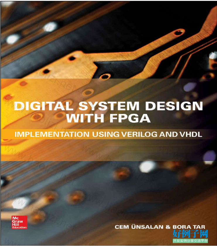
【实例简介】Digital System Design with FPGA Implementation Using Verilog and VHDL
讲FPGA很全面的一本书,从FPGA内部结构,到硬件描述语言,到具体的设计单元,再到综合应用。值得研究。
【实例截图】
【核心代码】
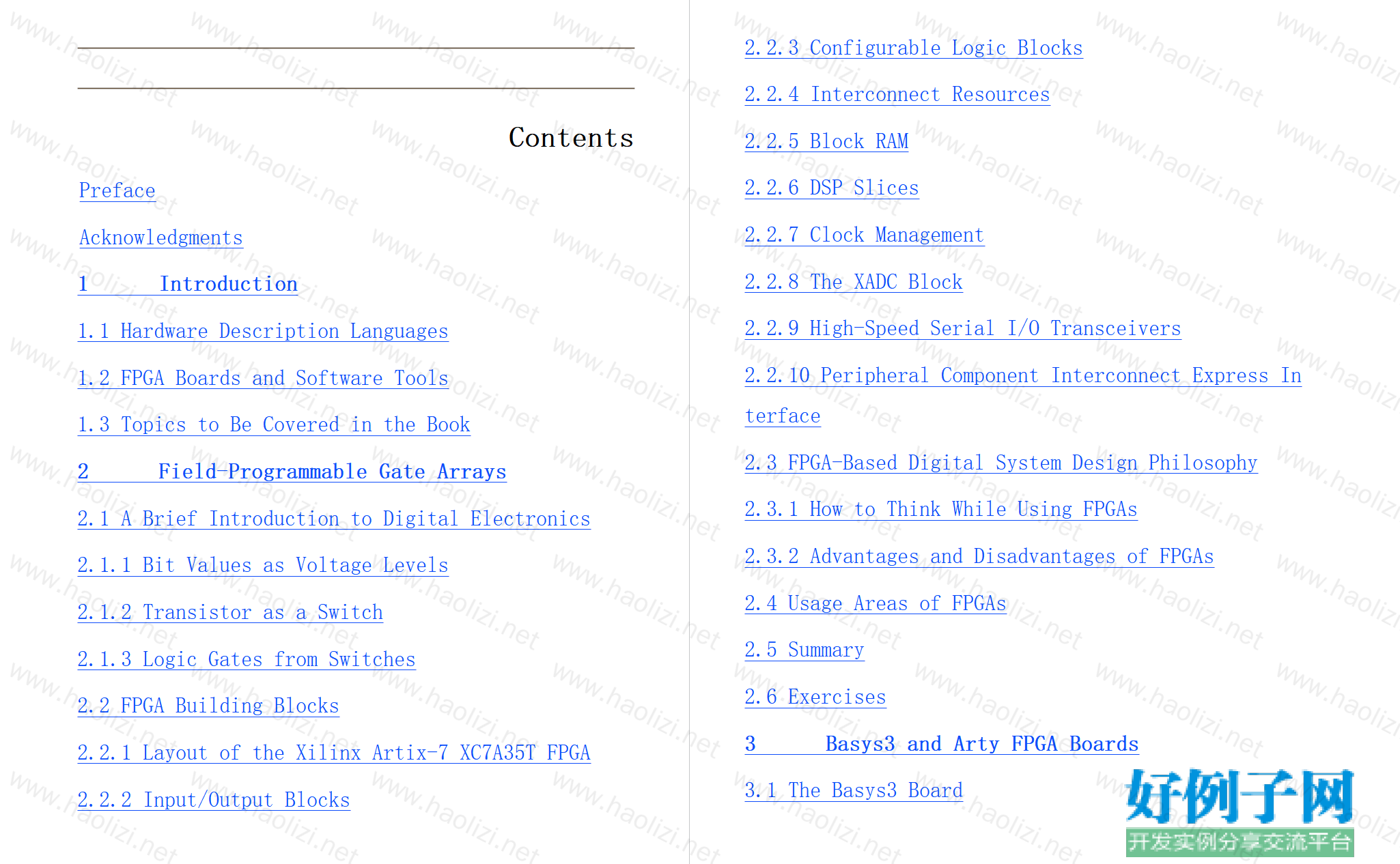
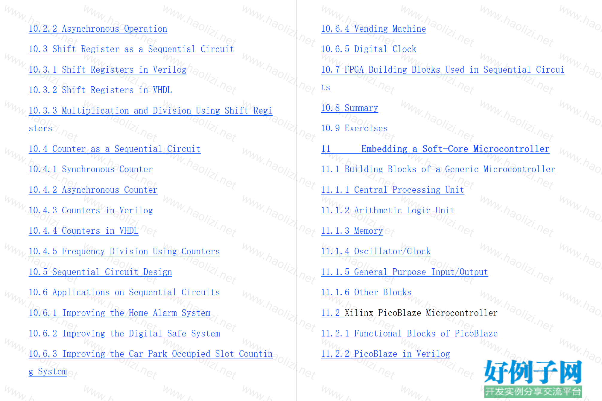
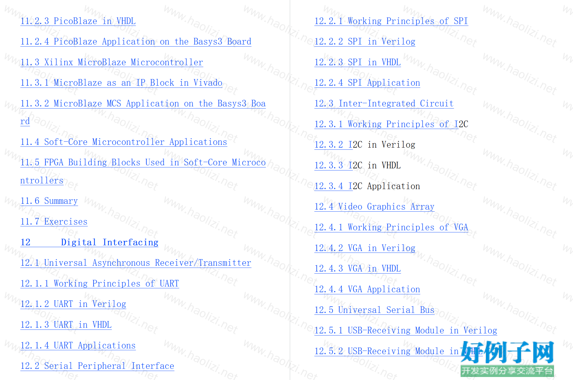
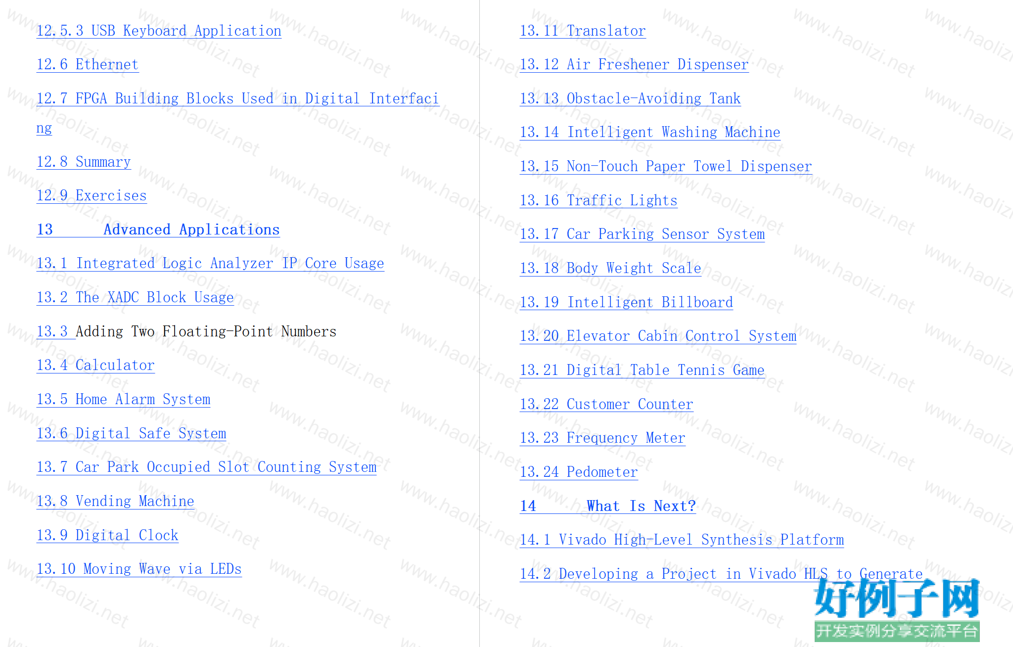
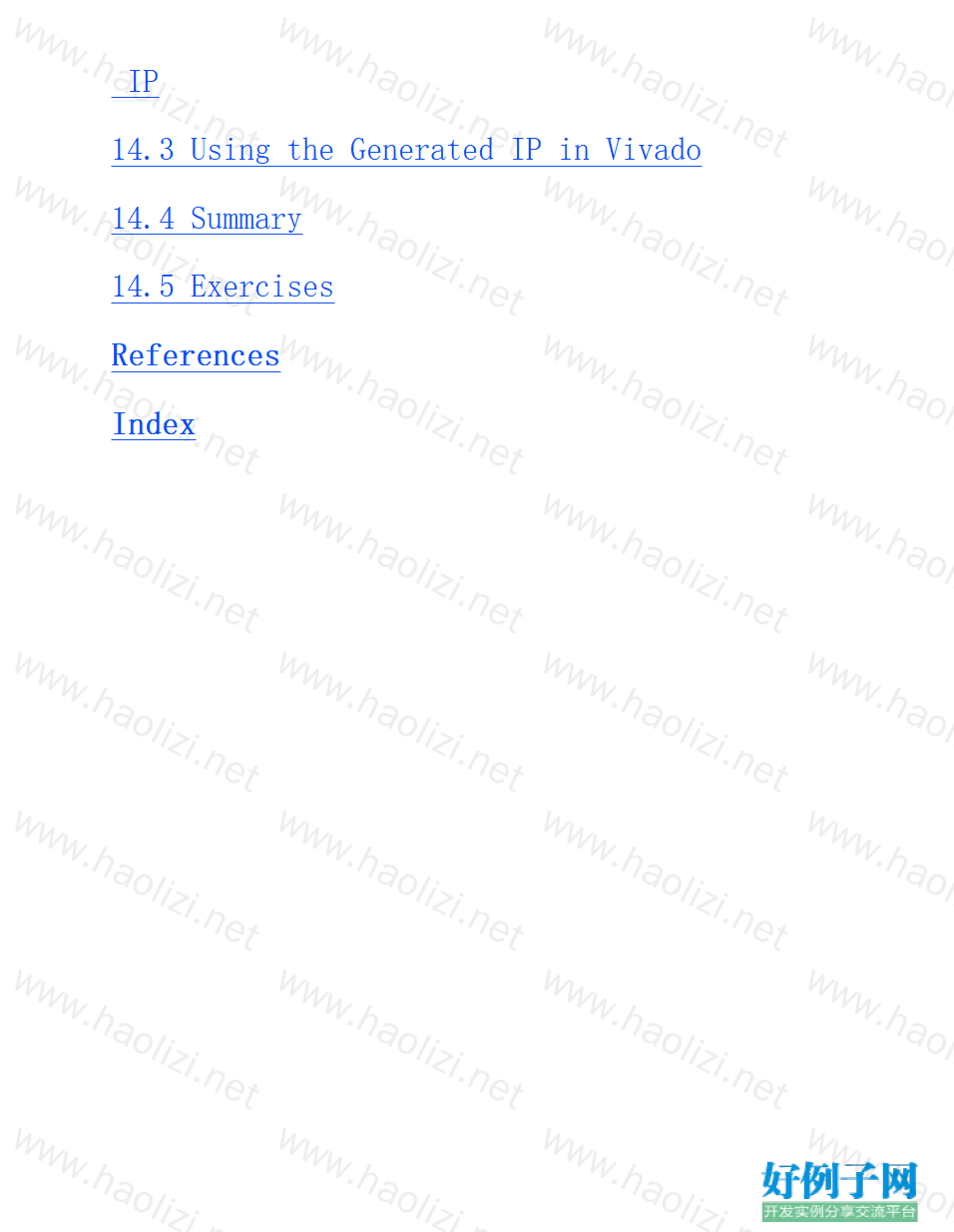
Contents
Preface
Acknowledgments
1 Introduction
1.1 Hardware Description Languages
1.2 FPGA Boards and Software Tools
1.3 Topics to Be Covered in the Book
2 Field-Programmable Gate Arrays
2.1 A Brief Introduction to Digital Electronics
2.1.1 Bit Values as Voltage Levels
2.1.2 Transistor as a Switch
2.1.3 Logic Gates from Switches
2.2 FPGA Building Blocks
2.2.1 Layout of the Xilinx Artix-7 XC7A35T FPGA
2.2.2 Input/Output Blocks
2.2.3 Configurable Logic Blocks
2.2.4 Interconnect Resources
2.2.5 Block RAM
2.2.6 DSP Slices
2.2.7 Clock Management
2.2.8 The XADC Block
2.2.9 High-Speed Serial I/O Transceivers
2.2.10 Peripheral Component Interconnect Express Interface
2.3 FPGA-Based Digital System Design Philosophy
2.3.1 How to Think While Using FPGAs
2.3.2 Advantages and Disadvantages of FPGAs
2.4 Usage Areas of FPGAs
2.5 Summary
2.6 Exercises
3 Basys3 and Arty FPGA Boards
3.1 The Basys3 Board
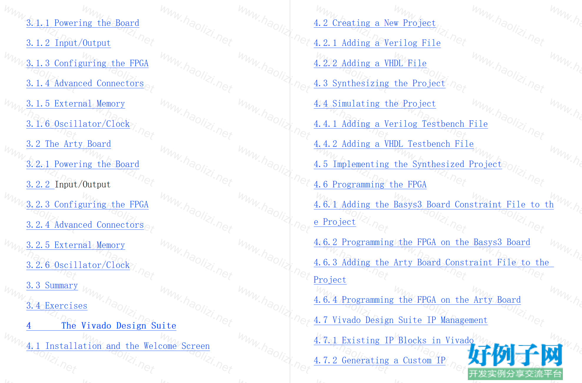
3.1.1 Powering the Board
3.1.2 Input/Output
3.1.3 Configuring the FPGA
3.1.4 Advanced Connectors
3.1.5 External Memory
3.1.6 Oscillator/Clock
3.2 The Arty Board
3.2.1 Powering the Board
3.2.2 Input/Output
3.2.3 Configuring the FPGA
3.2.4 Advanced Connectors
3.2.5 External Memory
3.2.6 Oscillator/Clock
3.3 Summary
3.4 Exercises
4 The Vivado Design Suite
4.1 Installation and the Welcome Screen
4.2 Creating a New Project
4.2.1 Adding a Verilog File
4.2.2 Adding a VHDL File
4.3 Synthesizing the Project
4.4 Simulating the Project
4.4.1 Adding a Verilog Testbench File
4.4.2 Adding a VHDL Testbench File
4.5 Implementing the Synthesized Project
4.6 Programming the FPGA
4.6.1 Adding the Basys3 Board Constraint File to the Project
4.6.2 Programming the FPGA on the Basys3 Board
4.6.3 Adding the Arty Board Constraint File to the Project
4.6.4 Programming the FPGA on the Arty Board
4.7 Vivado Design Suite IP Management
4.7.1 Existing IP Blocks in Vivado
4.7.2 Generating a Custom IP
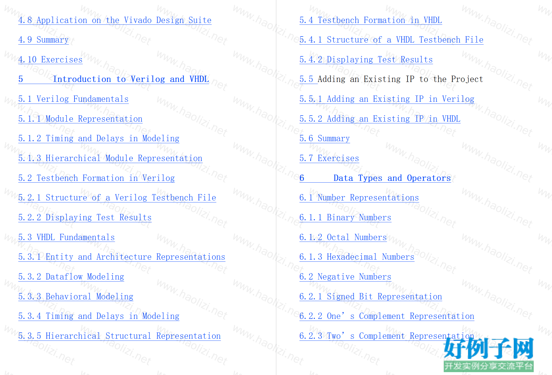
4.8 Application on the Vivado Design Suite
4.9 Summary
4.10 Exercises
5 Introduction to Verilog and VHDL
5.1 Verilog Fundamentals
5.1.1 Module Representation
5.1.2 Timing and Delays in Modeling
5.1.3 Hierarchical Module Representation
5.2 Testbench Formation in Verilog
5.2.1 Structure of a Verilog Testbench File
5.2.2 Displaying Test Results
5.3 VHDL Fundamentals
5.3.1 Entity and Architecture Representations
5.3.2 Dataflow Modeling
5.3.3 Behavioral Modeling
5.3.4 Timing and Delays in Modeling
5.3.5 Hierarchical Structural Representation
5.4 Testbench Formation in VHDL
5.4.1 Structure of a VHDL Testbench File
5.4.2 Displaying Test Results
5.5 Adding an Existing IP to the Project
5.5.1 Adding an Existing IP in Verilog
5.5.2 Adding an Existing IP in VHDL
5.6 Summary
5.7 Exercises
6 Data Types and Operators
6.1 Number Representations
6.1.1 Binary Numbers
6.1.2 Octal Numbers
6.1.3 Hexadecimal Numbers
6.2 Negative Numbers
6.2.1 Signed Bit Representation
6.2.2 One’s Complement Representation
6.2.3 Two’s Complement Representation
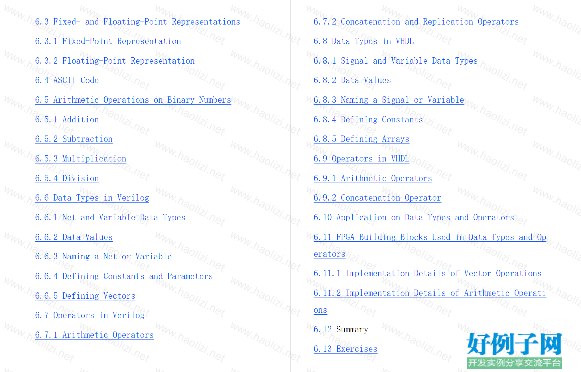
6.3 Fixed- and Floating-Point Representations
6.3.1 Fixed-Point Representation
6.3.2 Floating-Point Representation
6.4 ASCII Code
6.5 Arithmetic Operations on Binary Numbers
6.5.1 Addition
6.5.2 Subtraction
6.5.3 Multiplication
6.5.4 Division
6.6 Data Types in Verilog
6.6.1 Net and Variable Data Types
6.6.2 Data Values
6.6.3 Naming a Net or Variable
6.6.4 Defining Constants and Parameters
6.6.5 Defining Vectors
6.7 Operators in Verilog
6.7.1 Arithmetic Operators
6.7.2 Concatenation and Replication Operators
6.8 Data Types in VHDL
6.8.1 Signal and Variable Data Types
6.8.2 Data Values
6.8.3 Naming a Signal or Variable
6.8.4 Defining Constants
6.8.5 Defining Arrays
6.9 Operators in VHDL
6.9.1 Arithmetic Operators
6.9.2 Concatenation Operator
6.10 Application on Data Types and Operators
6.11 FPGA Building Blocks Used in Data Types and Operators
6.11.1 Implementation Details of Vector Operations
6.11.2 Implementation Details of Arithmetic Operations
6.12 Summary
6.13 Exercises
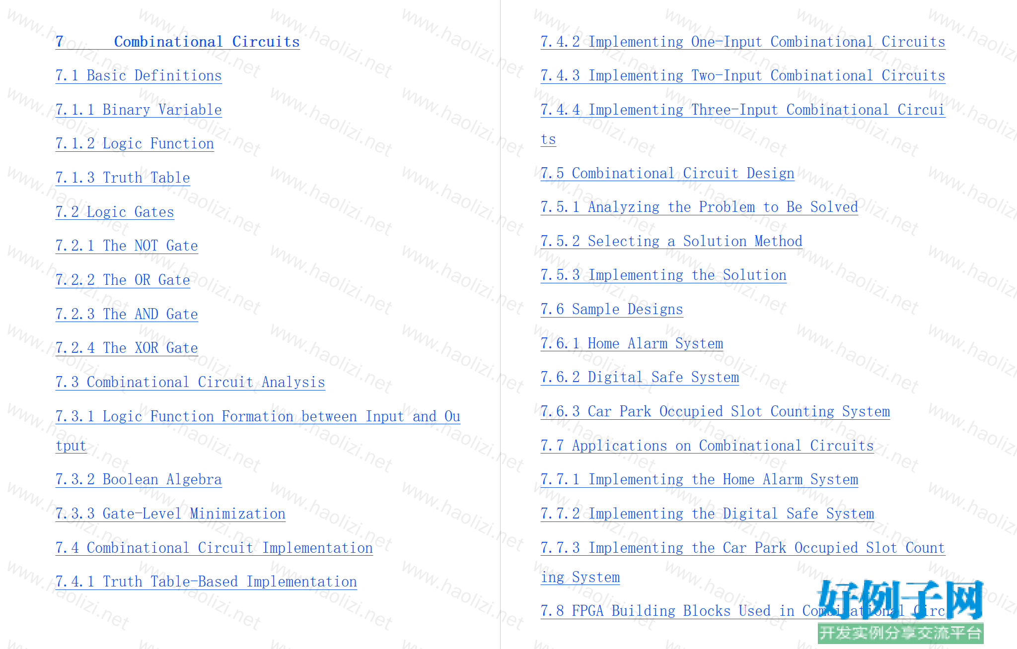
7 Combinational Circuits
7.1 Basic Definitions
7.1.1 Binary Variable
7.1.2 Logic Function
7.1.3 Truth Table
7.2 Logic Gates
7.2.1 The NOT Gate
7.2.2 The OR Gate
7.2.3 The AND Gate
7.2.4 The XOR Gate
7.3 Combinational Circuit Analysis
7.3.1 Logic Function Formation between Input and Output
7.3.2 Boolean Algebra
7.3.3 Gate-Level Minimization
7.4 Combinational Circuit Implementation
7.4.1 Truth Table-Based Implementation
7.4.2 Implementing One-Input Combinational Circuits
7.4.3 Implementing Two-Input Combinational Circuits
7.4.4 Implementing Three-Input Combinational Circuits
7.5 Combinational Circuit Design
7.5.1 Analyzing the Problem to Be Solved
7.5.2 Selecting a Solution Method
7.5.3 Implementing the Solution
7.6 Sample Designs
7.6.1 Home Alarm System
7.6.2 Digital Safe System
7.6.3 Car Park Occupied Slot Counting System
7.7 Applications on Combinational Circuits
7.7.1 Implementing the Home Alarm System
7.7.2 Implementing the Digital Safe System
7.7.3 Implementing the Car Park Occupied Slot Counting System
7.8 FPGA Building Blocks Used in Combinational Circuits
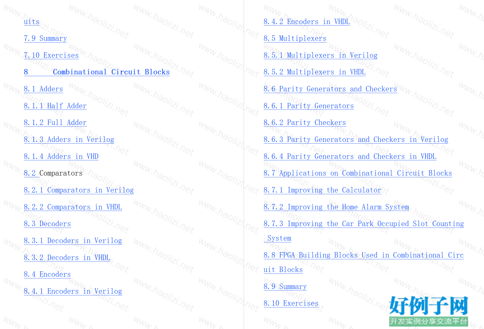
7.9 Summary
7.10 Exercises
8 Combinational Circuit Blocks
8.1 Adders
8.1.1 Half Adder
8.1.2 Full Adder
8.1.3 Adders in Verilog
8.1.4 Adders in VHD
8.2 Comparators
8.2.1 Comparators in Verilog
8.2.2 Comparators in VHDL
8.3 Decoders
8.3.1 Decoders in Verilog
8.3.2 Decoders in VHDL
8.4 Encoders
8.4.1 Encoders in Verilog
8.4.2 Encoders in VHDL
8.5 Multiplexers
8.5.1 Multiplexers in Verilog
8.5.2 Multiplexers in VHDL
8.6 Parity Generators and Checkers
8.6.1 Parity Generators
8.6.2 Parity Checkers
8.6.3 Parity Generators and Checkers in Verilog
8.6.4 Parity Generators and Checkers in VHDL
8.7 Applications on Combinational Circuit Blocks
8.7.1 Improving the Calculator
8.7.2 Improving the Home Alarm System
8.7.3 Improving the Car Park Occupied Slot Counting System
8.8 FPGA Building Blocks Used in Combinational Circuit Blocks
8.9 Summary
8.10 Exercises
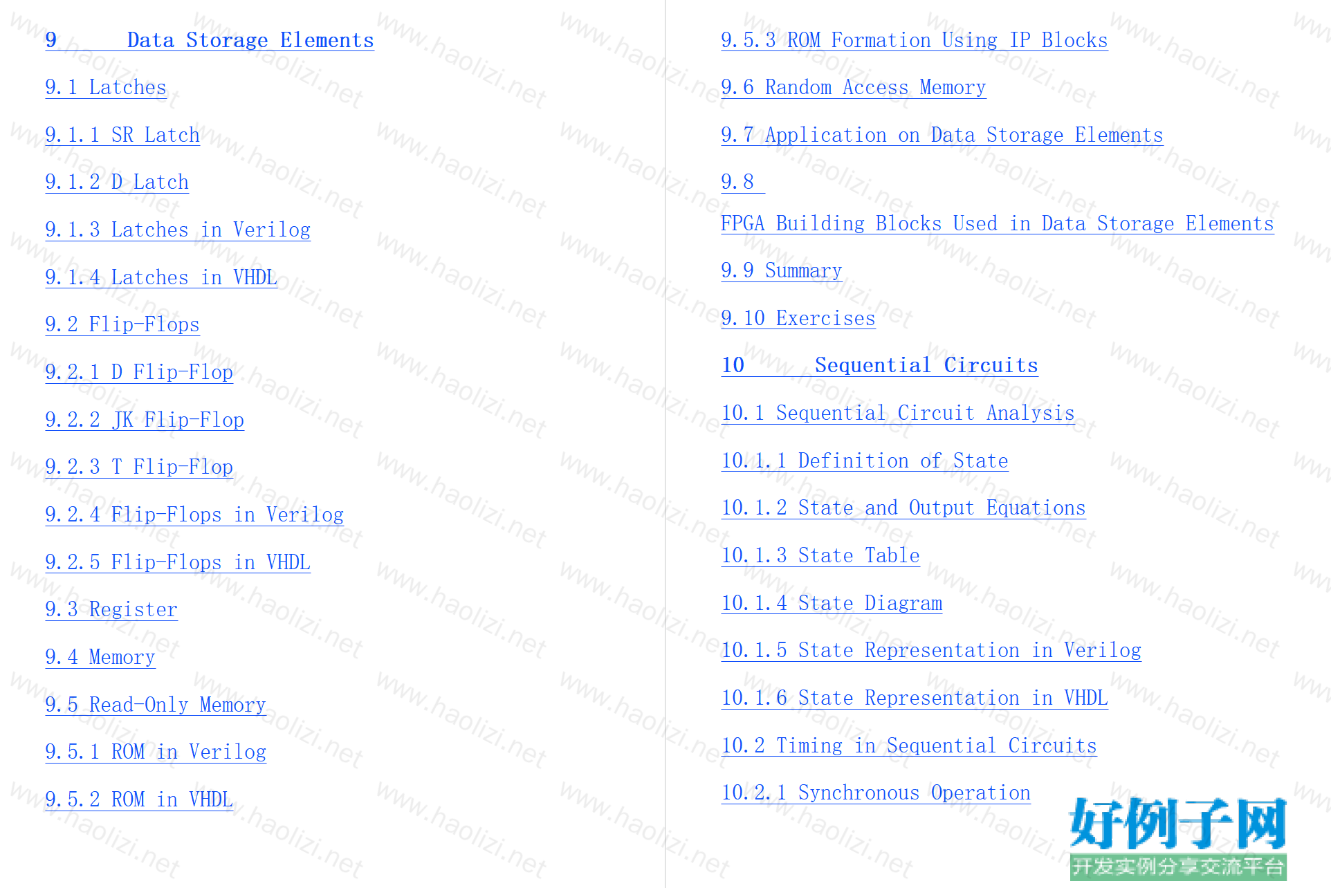
9 Data Storage Elements
9.1 Latches
9.1.1 SR Latch
9.1.2 D Latch
9.1.3 Latches in Verilog
9.1.4 Latches in VHDL
9.2 Flip-Flops
9.2.1 D Flip-Flop
9.2.2 JK Flip-Flop
9.2.3 T Flip-Flop
9.2.4 Flip-Flops in Verilog
9.2.5 Flip-Flops in VHDL
9.3 Register
9.4 Memory
9.5 Read-Only Memory
9.5.1 ROM in Verilog
9.5.2 ROM in VHDL
9.5.3 ROM Formation Using IP Blocks
9.6 Random Access Memory
9.7 Application on Data Storage Elements
9.8 FPGA Building Blocks Used in Data Storage Elements
9.9 Summary
9.10 Exercises
10 Sequential Circuits
10.1 Sequential Circuit Analysis
10.1.1 Definition of State
10.1.2 State and Output Equations
10.1.3 State Table
10.1.4 State Diagram
10.1.5 State Representation in Verilog
10.1.6 State Representation in VHDL
10.2 Timing in Sequential Circuits
10.2.1 Synchronous Operation
10.2.2 Asynchronous Operation
10.3 Shift Register as a Sequential Circuit
10.3.1 Shift Registers in Verilog
10.3.2 Shift Registers in VHDL
10.3.3 Multiplication and Division Using Shift Registers
10.4 Counter as a Sequential Circuit
10.4.1 Synchronous Counter
10.4.2 Asynchronous Counter
10.4.3 Counters in Verilog
10.4.4 Counters in VHDL
10.4.5 Frequency Division Using Counters
10.5 Sequential Circuit Design
10.6 Applications on Sequential Circuits
10.6.1 Improving the Home Alarm System
10.6.2 Improving the Digital Safe System
10.6.3 Improving the Car Park Occupied Slot Counting System
10.6.4 Vending Machine
10.6.5 Digital Clock
10.7 FPGA Building Blocks Used in Sequential Circuits
10.8 Summary
10.9 Exercises
11 Embedding a Soft-Core Microcontroller
11.1 Building Blocks of a Generic Microcontroller
11.1.1 Central Processing Unit
11.1.2 Arithmetic Logic Unit
11.1.3 Memory
11.1.4 Oscillator/Clock
11.1.5 General Purpose Input/Output
11.1.6 Other Blocks
11.2 Xilinx PicoBlaze Microcontroller
11.2.1 Functional Blocks of PicoBlaze
11.2.2 PicoBlaze in Verilog
11.2.3 PicoBlaze in VHDL
11.2.4 PicoBlaze Application on the Basys3 Board
11.3 Xilinx MicroBlaze Microcontroller
11.3.1 MicroBlaze as an IP Block in Vivado
11.3.2 MicroBlaze MCS Application on the Basys3 Board
11.4 Soft-Core Microcontroller Applications
11.5 FPGA Building Blocks Used in Soft-Core Microcontrollers
11.6 Summary
11.7 Exercises
12 Digital Interfacing
12.1 Universal Asynchronous Receiver/Transmitter
12.1.1 Working Principles of UART
12.1.2 UART in Verilog
12.1.3 UART in VHDL
12.1.4 UART Applications
12.2 Serial Peripheral Interface
12.2.1 Working Principles of SPI
12.2.2 SPI in Verilog
12.2.3 SPI in VHDL
12.2.4 SPI Application
12.3 Inter-Integrated Circuit
12.3.1 Working Principles of I2C
12.3.2 I2C in Verilog
12.3.3 I2C in VHDL
12.3.4 I2C Application
12.4 Video Graphics Array
12.4.1 Working Principles of VGA
12.4.2 VGA in Verilog
12.4.3 VGA in VHDL
12.4.4 VGA Application
12.5 Universal Serial Bus
12.5.1 USB-Receiving Module in Verilog
12.5.2 USB-Receiving Module in VHDL
12.5.3 USB Keyboard Application
12.6 Ethernet
12.7 FPGA Building Blocks Used in Digital Interfacing
12.8 Summary
12.9 Exercises
13 Advanced Applications
13.1 Integrated Logic Analyzer IP Core Usage
13.2 The XADC Block Usage
13.3 Adding Two Floating-Point Numbers
13.4 Calculator
13.5 Home Alarm System
13.6 Digital Safe System
13.7 Car Park Occupied Slot Counting System
13.8 Vending Machine
13.9 Digital Clock
13.10 Moving Wave via LEDs
13.11 Translator
13.12 Air Freshener Dispenser
13.13 Obstacle-Avoiding Tank
13.14 Intelligent Washing Machine
13.15 Non-Touch Paper Towel Dispenser
13.16 Traffic Lights
13.17 Car Parking Sensor System
13.18 Body Weight Scale
13.19 Intelligent Billboard
13.20 Elevator Cabin Control System
13.21 Digital Table Tennis Game
13.22 Customer Counter
13.23 Frequency Meter
13.24 Pedometer
14 What Is Next?
14.1 Vivado High-Level Synthesis Platform
14.2 Developing a Project in Vivado HLS to Generate IP
14.3 Using the Generated IP in Vivado
14.4 Summary
14.5 Exercises
References
Index
Digital System Design with FPGA Implementation Using Verilog and VHDL
相关软件
小贴士
感谢您为本站写下的评论,您的评论对其它用户来说具有重要的参考价值,所以请认真填写。
- 类似“顶”、“沙发”之类没有营养的文字,对勤劳贡献的楼主来说是令人沮丧的反馈信息。
- 相信您也不想看到一排文字/表情墙,所以请不要反馈意义不大的重复字符,也请尽量不要纯表情的回复。
- 提问之前请再仔细看一遍楼主的说明,或许是您遗漏了。
- 请勿到处挖坑绊人、招贴广告。既占空间让人厌烦,又没人会搭理,于人于己都无利。
关于好例子网
本站旨在为广大IT学习爱好者提供一个非营利性互相学习交流分享平台。本站所有资源都可以被免费获取学习研究。本站资源来自网友分享,对搜索内容的合法性不具有预见性、识别性、控制性,仅供学习研究,请务必在下载后24小时内给予删除,不得用于其他任何用途,否则后果自负。基于互联网的特殊性,平台无法对用户传输的作品、信息、内容的权属或合法性、安全性、合规性、真实性、科学性、完整权、有效性等进行实质审查;无论平台是否已进行审查,用户均应自行承担因其传输的作品、信息、内容而可能或已经产生的侵权或权属纠纷等法律责任。本站所有资源不代表本站的观点或立场,基于网友分享,根据中国法律《信息网络传播权保护条例》第二十二与二十三条之规定,若资源存在侵权或相关问题请联系本站客服人员,点此联系我们。关于更多版权及免责申明参见 版权及免责申明


网友评论
我要评论