
实例介绍
【实例简介】Gd32f405系列单片机
【实例截图】
【核心代码】
Table of Contents
Table of Contents ..................................................................................................... 1
List of Figures .......................................................................................................... 4
List of Tables ............................................................................................................ 5
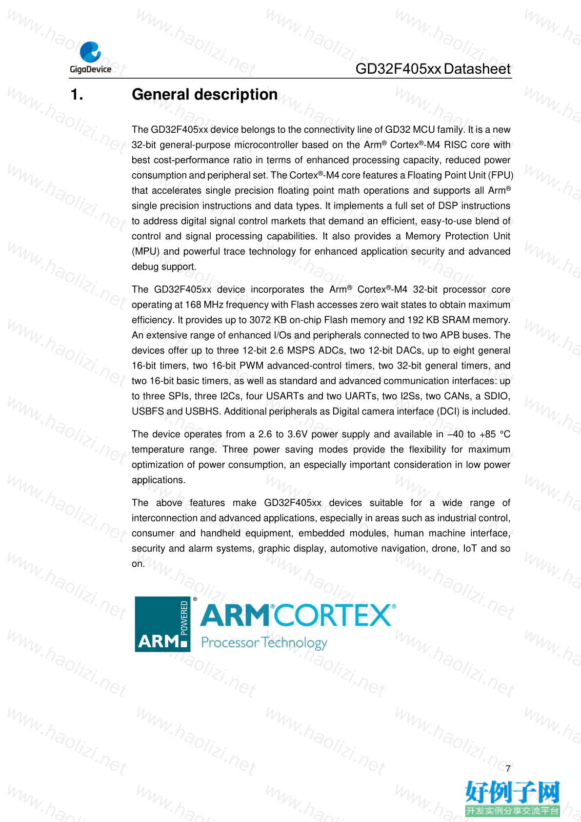
1. General description ........................................................................................... 7
2. Device overview ................................................................................................. 8
2.1. Device information ................................................................................................ 8
2.2. Block diagram........................................................................................................ 9
2.3. Pinouts and pin assignment............................................................................... 10
2.4. Memory map ........................................................................................................ 13
2.5. Clock tree............................................................................................................. 16
2.6. Pin definitions...................................................................................................... 17
2.6.1.
GD32F405Zx LQFP144 pin definitions ..........................................................................17
2.6.2.
GD32F405Vx LQFP100 pin definitions ..........................................................................25
2.6.3.
GD32F405Vx BGA100 pin definitions............................................................................31
2.6.4.
GD32F405Rx LQFP64 pin definitions............................................................................38
2.6.5.
GD32F405xx pin alternate functions..............................................................................43
3. Functional description..................................................................................... 50
3.1. Arm® Cortex®-M4 core......................................................................................... 50
3.2. On-chip memory.................................................................................................. 50
3.3. Clock, reset and supply management................................................................ 51
3.4. Boot modes.......................................................................................................... 52
3.5. Power saving modes........................................................................................... 52
3.6. Analog to digital converter (ADC) ...................................................................... 52
3.7. Digital to analog converter (DAC)....................................................................... 53
3.8. DMA...................................................................................................................... 53
3.9. General-purpose inputs/outputs (GPIOs) .......................................................... 54
3.10.
Timers and PWM generation ........................................................................... 54
3.11.
Real time clock (RTC) and backup registers.................................................. 55
3.12.
Inter-integrated circuit (I2C) ............................................................................ 56
3.13.
Serial peripheral interface (SPI) ...................................................................... 56
3.14.
Universal synchronous/asynchronous receiver transmitter (USART/UART)GD32F405xxDatasheet
2
56
3.15.
Inter-IC sound (I2S).......................................................................................... 57
3.16.
Universal serial bus full-speed interface (USBFS)......................................... 57
3.17.
Universal serial bus high-speed interface (USBHS) ...................................... 57
3.18.
Controller area network (CAN)........................................................................ 58
3.19.
Secure digital input and output card interface (SDIO)................................... 58
3.20.
Digital camera interface (DCI) ......................................................................... 58
3.21.
Debug mode ..................................................................................................... 58
3.22.
Package and operation temperature............................................................... 59
4. Electrical characteristics................................................................................. 60
4.1. Absolute maximum ratings................................................................................. 60
4.2. Operating conditions characteristics................................................................. 60
4.3. Power consumption ............................................................................................ 62
4.4. EMC characteristics ............................................................................................ 70
4.5. Power supply supervisor characteristics .......................................................... 70
4.6. Electrical sensitivity ............................................................................................ 72
4.7. External clock characteristics ............................................................................ 72
4.8. Internal clock characteristics ............................................................................. 75
4.9. PLL characteristics.............................................................................................. 76
4.10.
Memory characteristics ................................................................................... 78
4.11.
NRST pin characteristics................................................................................. 78
4.12.
GPIO characteristics........................................................................................ 79
4.13.
ADC characteristics ......................................................................................... 81
4.14.
Temperature sensor characteristics ............................................................... 83
4.15.
DAC characteristics ......................................................................................... 83
4.16.
I2C characteristics ........................................................................................... 84
4.17.
SPI characteristics ........................................................................................... 85
4.18.
I2S characteristics ........................................................................................... 87
4.19.
USART characteristics..................................................................................... 89
4.20.
SDIO characteristics ........................................................................................ 89
4.21.
CAN characteristics ......................................................................................... 89
4.22.
USBFS characteristics..................................................................................... 90GD32F405xxDatasheet
3
4.23.
USBHS characteristics .................................................................................... 91
4.24.
TIMER characteristics...................................................................................... 91
4.25.
DCI characteristics........................................................................................... 92
4.26.
WDGT characteristics...................................................................................... 92
4.27.
Parameter conditions....................................................................................... 92
5. Package information........................................................................................ 93
5.1. LQFP144 package outline dimensions .............................................................. 93
5.2. BGA100 package outline dimensions ................................................................ 95
5.3. LQFP100 package outline dimensions .............................................................. 97
5.4. LQFP64 package outline dimensions ................................................................ 99
5.5. Thermal characteristics .................................................................................... 101
6. Ordering information ..................................................................................... 103
7. Revision history ............................................................................................. 104GD32F405xxDatasheet
4
List of Figures
Figure 2-1. GD32F405xx block diagram..............................................................................................9
Figure 2-2. GD32F405Vx BGA100 pinouts........................................................................................10
Figure 2-3. GD32F405Zx LQFP144 pinouts ...................................................................................... 11
Figure 2-4. GD32F405Vx LQFP100 pinouts ......................................................................................12
Figure 2-5. GD32F405Rx LQFP64 pinouts ........................................................................................12
Figure 2-6. GD32F405xx clock tree ...................................................................................................16
Figure 4-1. Recommended power supply decoupling capacitors(1) (2)
...........................................61
Figure 4-2. Typical supply current consumption in Run mode......................................................67
Figure 4-3. Typical supply current consumption in Sleep mode ...................................................68
Figure 4-4. Recommended PDR_ON pin circuit...............................................................................72
Figure 4-5. Recommended external NRST pin circuit(1)
..................................................................79
Figure 4-6. I/O port AC characteristics definition ............................................................................80
Figure 4-7. I2C bus timing diagram ...................................................................................................85
Figure 4-8. SPI timing diagram - master mode ................................................................................86
Figure 4-9. SPI timing diagram - slave mode ...................................................................................86
Figure 4-10. I2S timing diagram - master mode...............................................................................88
Figure 4-11. I2S timing diagram - slave mode..................................................................................88
Figure 4-12. USBFS timings: definition of data signal rise and fall time ......................................90
Figure 5-1. LQFP144 package outline ...............................................................................................93
Figure 5-2. LQFP144 recommended footprint..................................................................................94
Figure 5-3. BGA100 package outline.................................................................................................95
Figure 5-4. BGA100 recommended footprint ...................................................................................96
Figure 5-5. LQFP100 package outline ...............................................................................................97
Figure 5-6. LQFP100 recommended footprint..................................................................................98
Figure 5-7. LQFP64 package outline .................................................................................................99
Figure 5-8. LQFP64 recommended footprint..................................................................................100GD32F405xxDatasheet
5
List of Tables
Table 2-1. GD32F405xx devices features and peripheral list ...........................................................8
Table 2-2. GD32F405xx memory map ...............................................................................................13
Table 2-3. GD32F405Zx LQFP144 pin definitions ............................................................................17
Table 2-4. GD32F405Vx LQFP100 pin definitions ............................................................................25
Table 2-5. GD32F405Vx BGA100 pin definitions..............................................................................31
Table 2-6. GD32F405Rx LQFP64 pin definitions..............................................................................38
Table 2-7. Port A alternate functions summary ...............................................................................43
Table 2-8. Port B alternate functions summary ...............................................................................44
Table 2-9. Port C alternate functions summary ...............................................................................45
Table 2-10. Port D alternate functions summary .............................................................................46
Table 2-11. Port E alternate functions summary .............................................................................47
Table 2-12. Port F alternate functions summary..............................................................................48
Table 2-13. Port G alternate functions summary .............................................................................48
Table 4-1. Absolute maximum ratings(1)(4)
........................................................................................60
Table 4-2. DC operating conditions...................................................................................................60
Table 4-3. Clock frequency(1)
..............................................................................................................61
Table 4-4. Operating conditions at Power up / Power down(1)
........................................................61
Table 4-5. Start-up timings of Operating conditions(1)(2)(3)
..............................................................61
Table 4-6. Power saving mode wakeup timings characteristics(1)(2)
..............................................62
Table 4-7. Power consumption characteristics(2)(3)(4)(5)
....................................................................62
Table 4-8. Peripheral current consumption characteristics(1)
........................................................68
Table 4-9. EMS characteristics(1)
.......................................................................................................70
Table 4-10. EMI characteristics(1)
.......................................................................................................70
Table 4-11. Power supply supervisor characteristics .....................................................................70
Table 4-12. ESD characteristics(1)
......................................................................................................72
Table 4-13. Static latch-up characteristics(1)
....................................................................................72
Table 4-14. High speed external clock (HXTAL) generated from a crystal/ceramic
characteristics.....................................................................................................................................72
Table 4-15. High speed external clock characteristics (HXTAL in bypass mode)........................73
Table 4-16. Low speed external clock (LXTAL) generated from a crystal/ceramic characteristics
..............................................................................................................................................................73
Table 4-17. Low speed external user clock characteristics (LXTAL in bypass mode) ................74
Table 4-18. High speed internal clock (IRC16M) characteristics....................................................75
Table 4-19. High speed internal clock (IRC48M) characteristics....................................................75
Table 4-20. Low speed internal clock (IRC32K) characteristics.....................................................76
Table 4-21. PLL characteristics .........................................................................................................76
Table 4-22. PLLI2S characteristics....................................................................................................77
Table 4-23. PLLSAI characteristics ...................................................................................................77
Table 4-24. PLL spread spectrum clock generation (SSCG) characteristics................................77
Table 4-25. Flash memory characteristics........................................................................................78
Table 4-26. NRST pin characteristics................................................................................................78GD32F405xxDatasheet
6
Table 4-27. I/O port DC characteristics(1)(3)
.......................................................................................79
Table 4-28. I/O port AC characteristics(1)(2)
.......................................................................................80
Table 4-29. ADC characteristics ........................................................................................................81
Table 4-30. ADC RAIN max for fADC = 40 MHz(2)
................................................................................81
Table 4-31. ADC dynamic accuracy at fADC = 30 MHz(1)
...................................................................82
Table 4-32. ADC dynamic accuracy at fADC = 30 MHz(1)
...................................................................82
Table 4-33. ADC dynamic accuracy at fADC = 36 MHz(1)
...................................................................82
Table 4-34. ADC dynamic accuracy at fADC = 40 MHz(1)
...................................................................82
Table 4-35. ADC static accuracy at fADC = 15 MHz(1)
.........................................................................82
Table 4-36. Temperature sensor characteristics(1)
..........................................................................83
Table 4-37. DAC characteristics ........................................................................................................83
Table 4-38. I2C characteristics(1)(2)
.....................................................................................................84
Table 4-39. Standard SPI characteristics(1)
.......................................................................................85
Table 4-40. I2S characteristics(1)(2)
.....................................................................................................87
Table 4-41. USART characteristics(1)
.................................................................................................89
Table 4-42. SDIO characteristics(1)(2)
..................................................................................................89
Table 4-43. USBFS start up time........................................................................................................90
Table 4-44. USBFS DC electrical characteristics.............................................................................90
Table 4-45. USBFS full speed-electrical characteristics(1)
..............................................................90
Table 4-46. TIMER characteristics(1)
..................................................................................................91
Table 4-47. DCI characteristics(1)
.......................................................................................................92
Table 4-48. FWDGT min/max timeout period at 32 kHz (IRC32K)(1)
................................................92
Table 4-49. WWDGT min-max timeout value at 42 MHz (fPCLK1)
(1)
...................................................92
Table 5-1. LQFP144 package dimensions ........................................................................................93
Table 5-2. BGA100 package dimensions ..........................................................................................95
Table 5-3. LQFP100 package dimensions ........................................................................................97
Table 5-4. LQFP64 package dimensions ..........................................................................................99
Table 5-5. Package thermal characteristics(1)
................................................................................101
Table 6-1. Part ordering code for GD32F405xx devices................................................................103
Table 7-1. Revision history...............................................................................................................104
好例子网口号:伸出你的我的手 — 分享!
小贴士
感谢您为本站写下的评论,您的评论对其它用户来说具有重要的参考价值,所以请认真填写。
- 类似“顶”、“沙发”之类没有营养的文字,对勤劳贡献的楼主来说是令人沮丧的反馈信息。
- 相信您也不想看到一排文字/表情墙,所以请不要反馈意义不大的重复字符,也请尽量不要纯表情的回复。
- 提问之前请再仔细看一遍楼主的说明,或许是您遗漏了。
- 请勿到处挖坑绊人、招贴广告。既占空间让人厌烦,又没人会搭理,于人于己都无利。
关于好例子网
本站旨在为广大IT学习爱好者提供一个非营利性互相学习交流分享平台。本站所有资源都可以被免费获取学习研究。本站资源来自网友分享,对搜索内容的合法性不具有预见性、识别性、控制性,仅供学习研究,请务必在下载后24小时内给予删除,不得用于其他任何用途,否则后果自负。基于互联网的特殊性,平台无法对用户传输的作品、信息、内容的权属或合法性、安全性、合规性、真实性、科学性、完整权、有效性等进行实质审查;无论平台是否已进行审查,用户均应自行承担因其传输的作品、信息、内容而可能或已经产生的侵权或权属纠纷等法律责任。本站所有资源不代表本站的观点或立场,基于网友分享,根据中国法律《信息网络传播权保护条例》第二十二与二十三条之规定,若资源存在侵权或相关问题请联系本站客服人员,点此联系我们。关于更多版权及免责申明参见 版权及免责申明

网友评论
我要评论