
实例介绍
【实例简介】PCIe标准规范5.0
【实例截图】
【实例截图】


【核心代码】
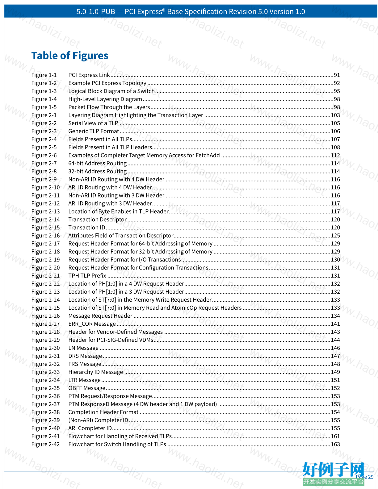
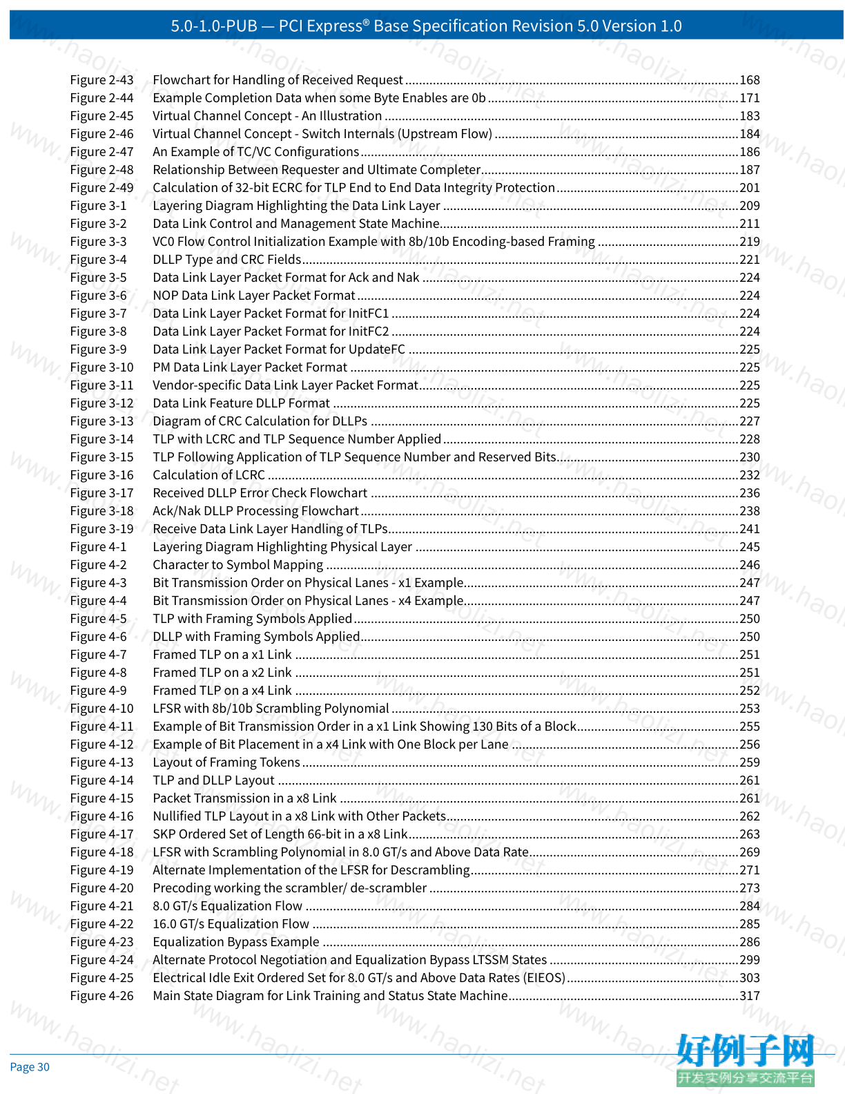
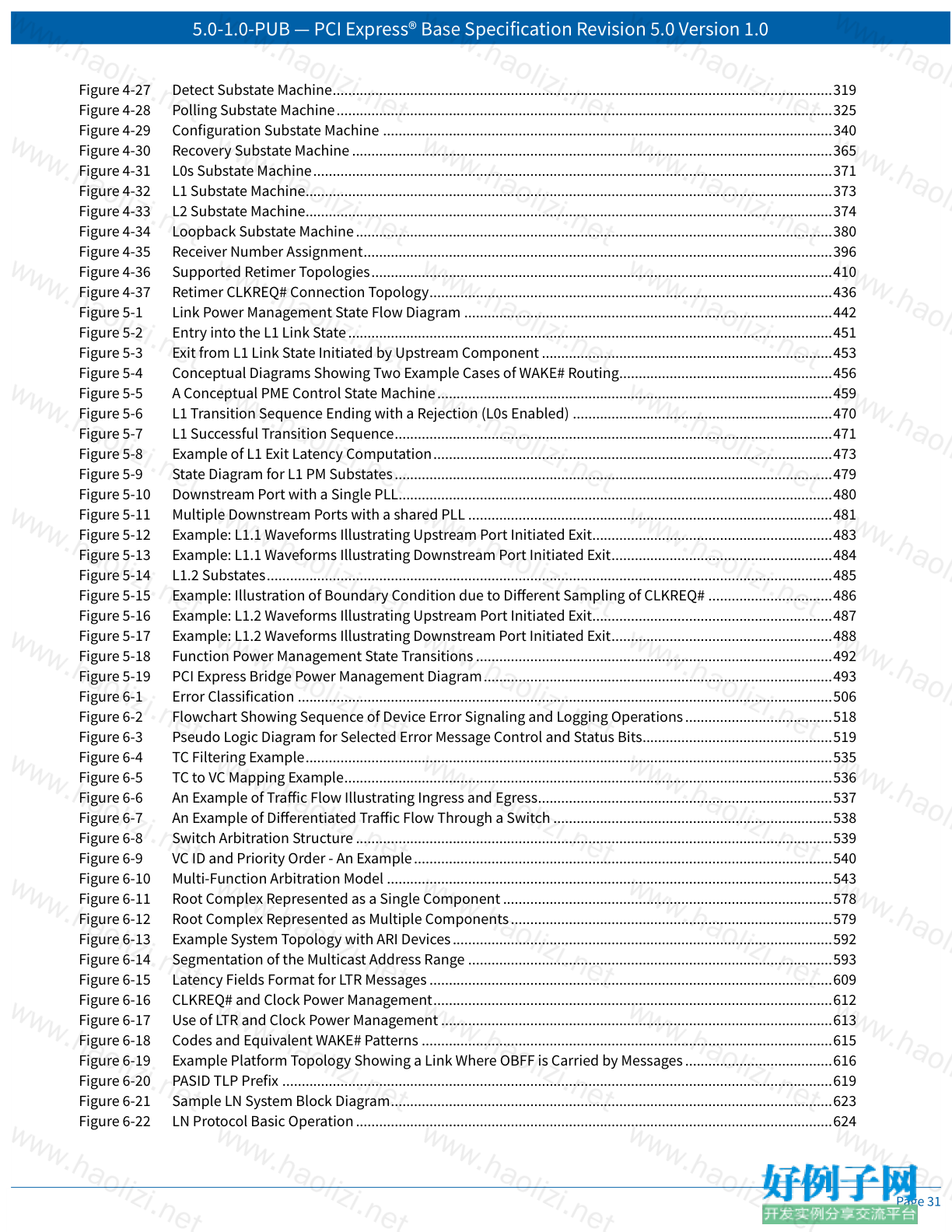
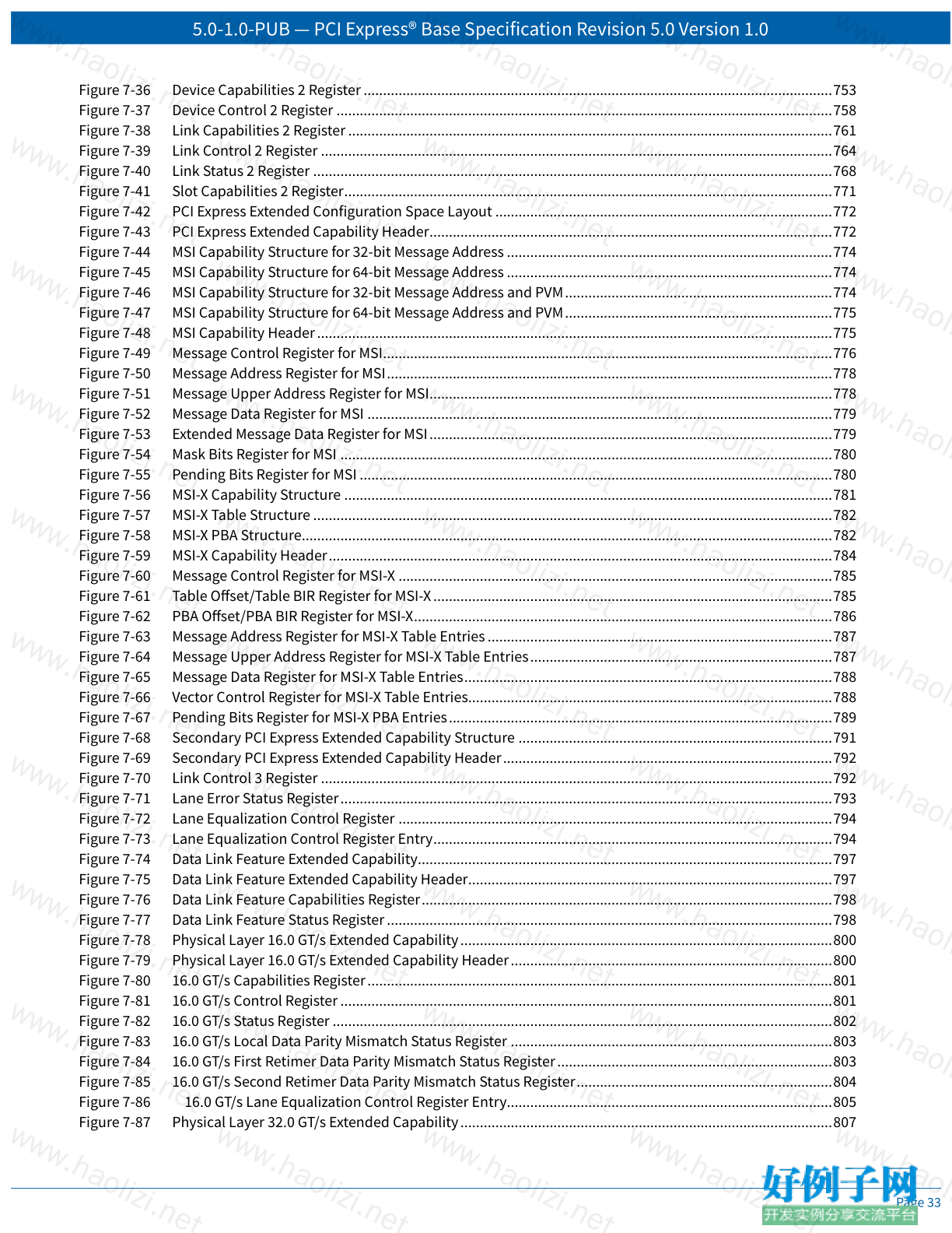
Table of Contents
1.
Introduction.......................................................................................................................................................................89
1.1 A Third Generation I/O Interconnect.................................................................................................................................89
1.2 PCI Express Link.................................................................................................................................................................90
1.3 PCI Express Fabric Topology .............................................................................................................................................92
1.3.1 Root Complex ............................................................................................................................................................92
1.3.2 Endpoints...................................................................................................................................................................93
1.3.2.1
Legacy Endpoint Rules ......................................................................................................................................93
1.3.2.2
PCI Express Endpoint Rules...............................................................................................................................94
1.3.2.3
Root Complex Integrated Endpoint Rules ........................................................................................................94
1.3.3 Switch.........................................................................................................................................................................95
1.3.4 Root Complex Event Collector ..................................................................................................................................96
1.3.5 PCI Express to PCI/PCI-X Bridge ................................................................................................................................96
1.4 Hardware/Software Model for Discovery, Configuration and Operation........................................................................96
1.5 PCI Express Layering Overview.........................................................................................................................................97
1.5.1 Transaction Layer ......................................................................................................................................................99
1.5.2 Data Link Layer ..........................................................................................................................................................99
1.5.3 Physical Layer............................................................................................................................................................99
1.5.4 Layer Functions and Services .................................................................................................................................100
1.5.4.1 Transaction Layer Services .............................................................................................................................100
1.5.4.2
Data Link Layer Services..................................................................................................................................101
1.5.4.3
Physical Layer Services ...................................................................................................................................101
1.5.4.4
Inter-Layer Interfaces ......................................................................................................................................102
1.5.4.4.1
Transaction/Data Link Interface..............................................................................................................102
1.5.4.4.2
Data Link/Physical Interface ...................................................................................................................102
2. Transaction Layer Specification......................................................................................................................................103
2.1 Transaction Layer Overview............................................................................................................................................103
2.1.1 Address Spaces, Transaction Types, and Usage.....................................................................................................104
2.1.1.1
Memory Transactions ......................................................................................................................................104
2.1.1.2
I/O Transactions...............................................................................................................................................104
2.1.1.3
Configuration Transactions.............................................................................................................................105
2.1.1.4
Message Transactions .....................................................................................................................................105
2.1.2 Packet Format Overview .........................................................................................................................................105
2.2 Transaction Layer Protocol - Packet Definition..............................................................................................................107
2.2.1 Common Packet Header Fields...............................................................................................................................107
2.2.2 TLPs with Data Payloads - Rules .............................................................................................................................110
2.2.3 TLP Digest Rules ......................................................................................................................................................113
2.2.4 Routing and Addressing Rules ................................................................................................................................113
2.2.4.1 Address-Based Routing Rules .........................................................................................................................113
2.2.4.2
ID Based Routing Rules ...................................................................................................................................115
2.2.5 First/Last DW Byte Enables Rules............................................................................................................................117
2.2.6 Transaction Descriptor............................................................................................................................................119
2.2.6.1 Overview ..........................................................................................................................................................119
2.2.6.2 Transaction Descriptor - Transaction ID Field ................................................................................................120
2.2.6.3
Transaction Descriptor - Attributes Field........................................................................................................125
2.2.6.4
Relaxed Ordering and ID-Based Ordering Attributes .....................................................................................126
2.2.6.5
No Snoop Attribute..........................................................................................................................................126
5.0-1.0-PUB — PCI Express® Base Specification Revision 5.0 Version 1.0
Page 32.2.6.6 Transaction Descriptor - Traffic Class Field ....................................................................................................127
2.2.7 Memory, I/O, and Configuration Request Rules .....................................................................................................127
2.2.7.1 TPH Rules.........................................................................................................................................................131
2.2.8 Message Request Rules ...........................................................................................................................................133
2.2.8.1
INTx Interrupt Signaling - Rules ......................................................................................................................135
2.2.8.2
Power Management Messages........................................................................................................................139
2.2.8.3
Error Signaling Messages ................................................................................................................................140
2.2.8.4
Locked Transactions Support .........................................................................................................................141
2.2.8.5
Slot Power Limit Support................................................................................................................................142
2.2.8.6 Vendor_Defined Messages ..............................................................................................................................143
2.2.8.6.1
PCI-SIG-Defined VDMs .............................................................................................................................144
2.2.8.6.2
LN Messages.............................................................................................................................................145
2.2.8.6.3
Device Readiness Status (DRS) Message.................................................................................................146
2.2.8.6.4
Function Readiness Status Message (FRS Message) ..............................................................................147
2.2.8.6.5
Hierarchy ID Message ..............................................................................................................................148
2.2.8.7
Ignored Messages ............................................................................................................................................150
2.2.8.8
Latency Tolerance Reporting (LTR) Message ..................................................................................................150
2.2.8.9
Optimized Buffer Flush/Fill (OBFF) Message..................................................................................................151
2.2.8.10 Precision Time Measurement (PTM) Messages ..............................................................................................152
2.2.9 Completion Rules ....................................................................................................................................................153
2.2.10 TLP Prefix Rules .......................................................................................................................................................156
2.2.10.1 Local TLP Prefix Processing.............................................................................................................................157
2.2.10.1.1 Vendor Defined Local TLP Prefix.............................................................................................................157
2.2.10.2 End-End TLP Prefix Processing .......................................................................................................................157
2.2.10.2.1 Vendor Defined End-End TLP Prefix .......................................................................................................159
2.2.10.2.2 Root Ports with End-End TLP Prefix Supported.....................................................................................159
2.3 Handling of Received TLPs..............................................................................................................................................160
2.3.1 Request Handling Rules ..........................................................................................................................................163
2.3.1.1
Data Return for Read Requests .......................................................................................................................169
2.3.2 Completion Handling Rules ....................................................................................................................................175
2.4 Transaction Ordering.......................................................................................................................................................177
2.4.1 Transaction Ordering Rules.....................................................................................................................................177
2.4.2 Update Ordering and Granularity Observed by a Read Transaction.....................................................................181
2.4.3 Update Ordering and Granularity Provided by a Write Transaction .....................................................................182
2.5 Virtual Channel (VC) Mechanism.....................................................................................................................................182
2.5.1 Virtual Channel Identification (VC ID).....................................................................................................................184
2.5.2 TC to VC Mapping.....................................................................................................................................................185
2.5.3 VC and TC Rules .......................................................................................................................................................186
2.6 Ordering and Receive Buffer Flow Control .....................................................................................................................187
2.6.1 Flow Control Rules...................................................................................................................................................188
2.6.1.1
FC Information Tracked by Transmitter..........................................................................................................192
2.6.1.2
FC Information Tracked by Receiver...............................................................................................................194
2.7 Data Integrity ...................................................................................................................................................................198
2.7.1 ECRC Rules ...............................................................................................................................................................198
2.7.2 Error Forwarding .....................................................................................................................................................202
2.7.2.1
Error Forwarding Usage Model .......................................................................................................................202
2.7.2.2
Rules For Use of Data Poisoning .....................................................................................................................203
2.8 Completion Timeout Mechanism ...................................................................................................................................204
2.9 Link Status Dependencies ...............................................................................................................................................205
2.9.1 Transaction Layer Behavior in DL_Down Status ....................................................................................................205
5.0-1.0-PUB — PCI Express® Base Specification Revision 5.0 Version 1.0
Page 42.9.2 Transaction Layer Behavior in DL_Up Status .........................................................................................................206
2.9.3 Transaction Layer Behavior During Downstream Port Containment....................................................................206
3.
Data Link Layer Specification..........................................................................................................................................209
3.1 Data Link Layer Overview................................................................................................................................................209
3.2 Data Link Control and Management State Machine.......................................................................................................210
3.2.1 Data Link Control and Management State Machine Rules.....................................................................................211
3.3 Data Link Feature Exchange ............................................................................................................................................214
3.4 Flow Control Initialization Protocol................................................................................................................................215
3.4.1 Flow Control Initialization State Machine Rules.....................................................................................................215
3.4.2 Scaled Flow Control.................................................................................................................................................220
3.5 Data Link Layer Packets (DLLPs) .....................................................................................................................................221
3.5.1 Data Link Layer Packet Rules ..................................................................................................................................221
3.6 Data Integrity Mechansisms ............................................................................................................................................227
3.6.1 Introduction.............................................................................................................................................................227
3.6.2 LCRC, Sequence Number, and Retry Management (TLP Transmitter)..................................................................228
3.6.2.1
LCRC and Sequence Number Rules (TLP Transmitter) ..................................................................................228
3.6.2.2
Handling of Received DLLPs............................................................................................................................235
3.6.3 LCRC and Sequence Number (TLP Receiver)..........................................................................................................238
3.6.3.1
LCRC and Sequence Number Rules (TLP Receiver)........................................................................................239
4.
Physical Layer Logical Block ...........................................................................................................................................245
4.1 Introduction.....................................................................................................................................................................245
4.2 Logical Sub-block ............................................................................................................................................................245
4.2.1 Encoding for 2.5 GT/s and 5.0 GT/s Data Rates .......................................................................................................246
4.2.1.1 Symbol Encoding.............................................................................................................................................246
4.2.1.1.1
Serialization and De-serialization of Data ..............................................................................................246
4.2.1.1.2
Special Symbols for Framing and Link Management (K Codes)............................................................247
4.2.1.1.3
8b/10b Decode Rules...............................................................................................................................248
4.2.1.2
Framing and Application of Symbols to Lanes...............................................................................................249
4.2.1.3
Data Scrambling ..............................................................................................................................................252
4.2.2 Encoding for 8.0 GT/s and Higher Data Rates .........................................................................................................253
4.2.2.1
Lane Level Encoding........................................................................................................................................254
4.2.2.2
Ordered Set Blocks ..........................................................................................................................................256
4.2.2.2.1
Block Alignment ......................................................................................................................................256
4.2.2.3
Data Blocks ......................................................................................................................................................257
4.2.2.3.1
Framing Tokens .......................................................................................................................................258
4.2.2.3.2
Transmitter Framing Requirements........................................................................................................263
4.2.2.3.3
Receiver Framing Requirements.............................................................................................................264
4.2.2.3.4
Recovery from Framing Errors ................................................................................................................266
4.2.2.4
Scrambling.......................................................................................................................................................267
4.2.2.5
Precoding.........................................................................................................................................................272
4.2.2.6
Loopback with 128b/130b Code .....................................................................................................................274
4.2.3 Link Equalization Procedure for 8.0 GT/s and Higher Data Rates..........................................................................274
4.2.3.1
Rules for Transmitter Coefficients ..................................................................................................................286
4.2.3.2
Encoding of Presets .........................................................................................................................................287
4.2.4 Link Initialization and Training ...............................................................................................................................288
4.2.4.1 Training Sequences .........................................................................................................................................288
4.2.4.2 Alternate Protocol Negotiation .......................................................................................................................298
4.2.4.3
Electrical Idle Sequences (EIOS) .....................................................................................................................301
5.0-1.0-PUB — PCI Express® Base Specification Revision 5.0 Version 1.0
Page 54.2.4.4
Inferring Electrical Idle ....................................................................................................................................305
4.2.4.5
Lane Polarity Inversion....................................................................................................................................306
4.2.4.6
Fast Training Sequence (FTS)..........................................................................................................................306
4.2.4.7
Start of Data Stream Ordered Set (SDS Ordered Set).....................................................................................308
4.2.4.8
Link Error Recovery .........................................................................................................................................309
4.2.4.9
Reset.................................................................................................................................................................309
4.2.4.9.1
Fundamental Reset .................................................................................................................................309
4.2.4.9.2
Hot Reset..................................................................................................................................................310
4.2.4.10 Link Data Rate Negotiation .............................................................................................................................310
4.2.4.11 Link Width and Lane Sequence Negotiation ..................................................................................................310
4.2.4.11.1 Required and Optional Port Behavior ....................................................................................................310
4.2.4.12 Lane-to-Lane De-skew.....................................................................................................................................311
4.2.4.13 Lane vs. Link Training......................................................................................................................................312
4.2.5 Link Training and Status State Machine (LTSSM) Descriptions..............................................................................312
4.2.5.1
Detect Overview ..............................................................................................................................................313
4.2.5.2
Polling Overview..............................................................................................................................................313
4.2.5.3
Configuration Overview ..................................................................................................................................313
4.2.5.4
Recovery Overview..........................................................................................................................................313
4.2.5.5
L0 Overview .....................................................................................................................................................314
4.2.5.6
L0s Overview....................................................................................................................................................314
4.2.5.7
L1 Overview .....................................................................................................................................................314
4.2.5.8
L2 Overview .....................................................................................................................................................314
4.2.5.9
Disabled Overview...........................................................................................................................................314
4.2.5.10 Loopback Overview.........................................................................................................................................314
4.2.5.11 Hot Reset Overview .........................................................................................................................................315
4.2.6 Link Training and Status State Rules ......................................................................................................................315
4.2.6.1
Detect...............................................................................................................................................................317
4.2.6.1.1
Detect.Quiet.............................................................................................................................................317
4.2.6.1.2
Detect.Active............................................................................................................................................318
4.2.6.2
Polling ..............................................................................................................................................................319
4.2.6.2.1
Polling.Active ...........................................................................................................................................319
4.2.6.2.2
Polling.Compliance .................................................................................................................................320
4.2.6.2.3
Polling.Configuration ..............................................................................................................................324
4.2.6.2.4
Polling.Speed...........................................................................................................................................325
4.2.6.3
Configuration...................................................................................................................................................325
4.2.6.3.1
Configuration.Linkwidth.Start................................................................................................................326
4.2.6.3.1.1
Downstream Lanes..........................................................................................................................326
4.2.6.3.1.2
Upstream Lanes...............................................................................................................................327
4.2.6.3.2
Configuration.Linkwidth.Accept.............................................................................................................329
4.2.6.3.2.1
Downstream Lanes..........................................................................................................................329
4.2.6.3.2.2
Upstream Lanes...............................................................................................................................330
4.2.6.3.3
Configuration.Lanenum.Accept..............................................................................................................332
4.2.6.3.3.1
Downstream Lanes..........................................................................................................................332
4.2.6.3.3.2
Upstream Lanes...............................................................................................................................333
4.2.6.3.4
Configuration.Lanenum.Wait..................................................................................................................333
4.2.6.3.4.1
Downstream Lanes..........................................................................................................................333
4.2.6.3.4.2
Upstream Lanes...............................................................................................................................334
4.2.6.3.5
Configuration.Complete..........................................................................................................................334
4.2.6.3.5.1
Downstream Lanes..........................................................................................................................334
4.2.6.3.5.2
Upstream Lanes...............................................................................................................................336
5.0-1.0-PUB — PCI Express® Base Specification Revision 5.0 Version 1.0
Page 64.2.6.3.6
Configuration.Idle....................................................................................................................................337
4.2.6.4
Recovery...........................................................................................................................................................340
4.2.6.4.1
Recovery.RcvrLock ..................................................................................................................................340
4.2.6.4.2
Recovery.Equalization.............................................................................................................................346
4.2.6.4.2.1
Downstream Lanes..........................................................................................................................347
4.2.6.4.2.1.1 Phase 1 of Transmitter Equalization.......................................................................................347
4.2.6.4.2.1.2 Phase 2 of Transmitter Equalization.......................................................................................349
4.2.6.4.2.1.3 Phase 3 of Transmitter Equalization.......................................................................................350
4.2.6.4.2.2
Upstream Lanes...............................................................................................................................352
4.2.6.4.2.2.1 Phase 0 of Transmitter Equalization.......................................................................................352
4.2.6.4.2.2.2 Phase 1 of Transmitter Equalization.......................................................................................353
4.2.6.4.2.2.3 Phase 2 of Transmitter Equalization.......................................................................................354
4.2.6.4.2.2.4 Phase 3 of Transmitter Equalization.......................................................................................356
4.2.6.4.3
Recovery.Speed .......................................................................................................................................357
4.2.6.4.4
Recovery.RcvrCfg.....................................................................................................................................358
4.2.6.4.5
Recovery.Idle ...........................................................................................................................................363
4.2.6.5
L0......................................................................................................................................................................366
4.2.6.6
L0s ....................................................................................................................................................................367
4.2.6.6.1
Receiver L0s .............................................................................................................................................368
4.2.6.6.1.1
Rx_L0s.Entry ....................................................................................................................................368
4.2.6.6.1.2
Rx_L0s.Idle.......................................................................................................................................368
4.2.6.6.1.3
Rx_L0s.FTS .......................................................................................................................................368
4.2.6.6.2
Transmitter L0s ........................................................................................................................................369
4.2.6.6.2.1
Tx_L0s.Entry ....................................................................................................................................369
4.2.6.6.2.2
Tx_L0s.Idle .......................................................................................................................................369
4.2.6.6.2.3
Tx_L0s.FTS .......................................................................................................................................369
4.2.6.7
L1......................................................................................................................................................................371
4.2.6.7.1
L1.Entry....................................................................................................................................................371
4.2.6.7.2
L1.Idle.......................................................................................................................................................371
4.2.6.8
L2......................................................................................................................................................................373
4.2.6.8.1
L2.Idle.......................................................................................................................................................373
4.2.6.8.2
L2.TransmitWake .....................................................................................................................................374
4.2.6.9
Disabled ...........................................................................................................................................................374
4.2.6.10 Loopback .........................................................................................................................................................375
4.2.6.10.1 Loopback.Entry .......................................................................................................................................375
4.2.6.10.2 Loopback.Active ......................................................................................................................................378
4.2.6.10.3 Loopback.Exit ..........................................................................................................................................379
4.2.6.11 Hot Reset..........................................................................................................................................................380
4.2.7 Clock Tolerance Compensation ..............................................................................................................................381
4.2.7.1 SKP Ordered Set for 8b/10b Encoding............................................................................................................382
4.2.7.2
SKP Ordered Set for 128b/130b Encoding......................................................................................................382
4.2.7.3
Rules for Transmitters .....................................................................................................................................386
4.2.7.4
Rules for Receivers...........................................................................................................................................387
4.2.8 Compliance Pattern in 8b/10b Encoding................................................................................................................388
4.2.9 Modified Compliance Pattern in 8b/10b Encoding ................................................................................................389
4.2.10 Compliance Pattern in 128b/130b Encoding..........................................................................................................390
4.2.11 Modified Compliance Pattern in 128b/130b Encoding ..........................................................................................393
4.2.12 Jitter Measurement Pattern in 128b/130b..............................................................................................................393
4.2.13 Lane Margining at Receiver.....................................................................................................................................394
4.2.13.1 Receiver Number, Margin Type, Usage Model, and Margin Payload Fields...................................................394
5.0-1.0-PUB — PCI Express® Base Specification Revision 5.0 Version 1.0
Page 74.2.13.1.1 Step Margin Execution Status .................................................................................................................399
4.2.13.1.2 Margin Payload for Step Margin Commands ..........................................................................................399
4.2.13.2 Margin Command and Response Flow...........................................................................................................400
4.2.13.3 Receiver Margin Testing Requirements ..........................................................................................................403
4.3 Retimers ...........................................................................................................................................................................407
4.3.1 Retimer Requirements ............................................................................................................................................408
4.3.2 Supported Retimer Topologies...............................................................................................................................409
4.3.3 Variables...................................................................................................................................................................410
4.3.4 Receiver Impedance Propagation Rules.................................................................................................................411
4.3.5 Switching Between Modes ......................................................................................................................................411
4.3.6 Forwarding Rules.....................................................................................................................................................411
4.3.6.1
Forwarding Type Rules....................................................................................................................................412
4.3.6.2
Orientation and Lane Numbers Rules ............................................................................................................412
4.3.6.3
Electrical Idle Exit Rules ..................................................................................................................................413
4.3.6.4
Data Rate Change and Determination Rules ..................................................................................................415
4.3.6.5
Electrical Idle Entry Rules................................................................................................................................416
4.3.6.6 Transmitter Settings Determination Rules .....................................................................................................417
4.3.6.7
Ordered Set Modification Rules ......................................................................................................................418
4.3.6.8
DLLP, TLP, and Logical Idle Modification Rules ..............................................................................................420
4.3.6.9
8b/10b Encoding Rules....................................................................................................................................421
4.3.6.10 8b/10b Scrambling Rules ................................................................................................................................421
4.3.6.11 Hot Reset Rules................................................................................................................................................421
4.3.6.12 Disable Link Rules............................................................................................................................................421
4.3.6.13 Loopback .........................................................................................................................................................422
4.3.6.14 Compliance Receive Rules ..............................................................................................................................423
4.3.6.15 Enter Compliance Rules ..................................................................................................................................424
4.3.7 Execution Mode Rules .............................................................................................................................................427
4.3.7.1 CompLoadBoard Rules....................................................................................................................................427
4.3.7.1.1
CompLoadBoard.Entry ...........................................................................................................................427
4.3.7.1.2
CompLoadBoard.Pattern ........................................................................................................................427
4.3.7.1.3
CompLoadBoard.Exit ..............................................................................................................................428
4.3.7.2
Link Equalization Rules ...................................................................................................................................429
4.3.7.2.1
Downstream Lanes ..................................................................................................................................429
4.3.7.2.1.1
Phase 2.............................................................................................................................................429
4.3.7.2.1.2
Phase 3 Active..................................................................................................................................429
4.3.7.2.1.3
Phase 3 Passive................................................................................................................................429
4.3.7.2.2
Upstream Lanes.......................................................................................................................................430
4.3.7.2.2.1
Phase 2 Active..................................................................................................................................430
4.3.7.2.2.2
Phase 2 Passive................................................................................................................................430
4.3.7.2.2.3
Phase 3.............................................................................................................................................430
4.3.7.2.3
Force Timeout..........................................................................................................................................431
4.3.7.3
Slave Loopback................................................................................................................................................431
4.3.7.3.1
Slave Loopback.Entry .............................................................................................................................431
4.3.7.3.2
Slave Loopback.Active ............................................................................................................................432
4.3.7.3.3
Slave Loopback.Exit ................................................................................................................................432
4.3.8 Retimer Latency.......................................................................................................................................................432
4.3.8.1
Measurement...................................................................................................................................................432
4.3.8.2
Maximum Limit on Retimer Latency...............................................................................................................432
4.3.8.3
Impacts on Upstream and Downstream Ports ...............................................................................................433
4.3.9 SRIS ..........................................................................................................................................................................433
5.0-1.0-PUB — PCI Express® Base Specification Revision 5.0 Version 1.0
Page 84.3.10 L1 PM Substates Support ........................................................................................................................................434
4.3.11 Retimer Configuration Parameters .........................................................................................................................436
4.3.11.1 Global Parameters ...........................................................................................................................................437
4.3.11.2 Per Physical Pseudo Port Parameters.............................................................................................................437
4.3.12 In Band Register Access ...........................................................................................................................................438
5.
Power Management.........................................................................................................................................................439
5.1 Overview ..........................................................................................................................................................................439
5.2 Link State Power Management .......................................................................................................................................440
5.3 PCI-PM Software Compatible Mechanisms ....................................................................................................................444
5.3.1 Device Power Management States (D-States) of a Function..................................................................................444
5.3.1.1
D0 State ............................................................................................................................................................445
5.3.1.2
D1 State ............................................................................................................................................................445
5.3.1.3
D2 State ............................................................................................................................................................445
5.3.1.4
D3 State ............................................................................................................................................................446
5.3.1.4.1
D3Hot State ...............................................................................................................................................447
5.3.1.4.2
D3Cold State..............................................................................................................................................448
5.3.2 PM Software Control of the Link Power Management State..................................................................................449
5.3.2.1
Entry into the L1 State.....................................................................................................................................450
5.3.2.2
Exit from L1 State.............................................................................................................................................453
5.3.2.3
Entry into the L2/L3 Ready State ....................................................................................................................454
5.3.3 Power Management Event Mechanisms.................................................................................................................454
5.3.3.1
Motivation ........................................................................................................................................................454
5.3.3.2
Link Wakeup.....................................................................................................................................................455
5.3.3.2.1
PME Synchronization...............................................................................................................................456
5.3.3.3
PM_PME Messages...........................................................................................................................................458
5.3.3.3.1
PM_PME “Backpressure” Deadlock Avoidance......................................................................................458
5.3.3.4
PME Rules.........................................................................................................................................................458
5.3.3.5
PM_PME Delivery State Machine.....................................................................................................................459
5.4 Native PCI Express Power Management Mechanisms ...................................................................................................460
5.4.1 Active State Power Management (ASPM) ...............................................................................................................460
5.4.1.1
L0s ASPM State.................................................................................................................................................462
5.4.1.1.1
Entry into the L0s State ...........................................................................................................................463
5.4.1.1.2
Exit from the L0s State.............................................................................................................................464
5.4.1.2
L1 ASPM State ..................................................................................................................................................464
5.4.1.2.1
ASPM Entry into the L1 State...................................................................................................................465
5.4.1.2.2
Exit from the L1 State ..............................................................................................................................471
5.4.1.3 ASPM Configuration.........................................................................................................................................474
5.4.1.3.1
Software Flow for Enabling or Disabling ASPM......................................................................................477
5.5 L1 PM Substates...............................................................................................................................................................478
5.5.1 Entry conditions for L1 PM Substates and L1.0 Requirements..............................................................................482
5.5.2 L1.1 Requirements...................................................................................................................................................483
5.5.2.1
Exit from L1.1 ...................................................................................................................................................483
5.5.3 L1.2 Requirements...................................................................................................................................................484
5.5.3.1
L1.2.Entry.........................................................................................................................................................485
5.5.3.2
L1.2.Idle............................................................................................................................................................486
5.5.3.3
L1.2.Exit............................................................................................................................................................486
5.5.3.3.1
Exit from L1.2 ...........................................................................................................................................487
5.5.4 L1 PM Substates Configuration...............................................................................................................................488
5.5.5 L1 PM Substates Timing Parameters ......................................................................................................................488
5.0-1.0-PUB — PCI Express® Base Specification Revision 5.0 Version 1.0
Page 95.5.6 Link Activation .........................................................................................................................................................489
5.6 Auxiliary Power Support..................................................................................................................................................490
5.7 Power Management System Messages and DLLPs ........................................................................................................490
5.8 PCI Function Power State Transitions.............................................................................................................................491
5.9 State Transition Recovery Time Requirements ..............................................................................................................492
5.10 PCI Bridges and Power Management..............................................................................................................................493
5.10.1 Switches and PCI Express to PCI Bridges................................................................................................................494
5.11 Power Management Events.............................................................................................................................................494
6. System Architecture ........................................................................................................................................................495
6.1 Interrupt and PME Support.............................................................................................................................................495
6.1.1 Rationale for PCI Express Interrupt Model..............................................................................................................495
6.1.2 PCI-compatible INTx Emulation..............................................................................................................................495
6.1.3 INTx Emulation Software Model..............................................................................................................................496
6.1.4 MSI and MSI-X Operation.........................................................................................................................................496
6.1.4.1
MSI Configuration............................................................................................................................................497
6.1.4.2
MSI-X Configuration.........................................................................................................................................498
6.1.4.3
Enabling Operation .........................................................................................................................................499
6.1.4.4
Sending Messages ...........................................................................................................................................500
6.1.4.5
Per-vector Masking and Function Masking.....................................................................................................500
6.1.4.6
Hardware/Software Synchronization .............................................................................................................501
6.1.4.7
Message Transaction Reception and Ordering Requirements ......................................................................503
6.1.5 PME Support............................................................................................................................................................503
6.1.6 Native PME Software Model ....................................................................................................................................503
6.1.7 Legacy PME Software Model ...................................................................................................................................504
6.1.8 Operating System Power Management Notification..............................................................................................504
6.1.9 PME Routing Between PCI Express and PCI Hierarchies........................................................................................504
6.2 Error Signaling and Logging............................................................................................................................................505
6.2.1 Scope........................................................................................................................................................................505
6.2.2 Error Classification ..................................................................................................................................................505
6.2.2.1 Correctable Errors ...........................................................................................................................................506
6.2.2.2
Uncorrectable Errors .......................................................................................................................................507
6.2.2.2.1
Fatal Errors...............................................................................................................................................507
6.2.2.2.2
Non-Fatal Errors.......................................................................................................................................507
6.2.3 Error Signaling .........................................................................................................................................................507
6.2.3.1 Completion Status...........................................................................................................................................507
6.2.3.2
Error Messages.................................................................................................................................................507
6.2.3.2.1
Uncorrectable Error Severity Programming (Advanced Error Reporting) ............................................509
6.2.3.2.2
Masking Individual Errors........................................................................................................................509
6.2.3.2.3
Error Pollution .........................................................................................................................................509
6.2.3.2.4
Advisory Non-Fatal Error Cases...............................................................................................................510
6.2.3.2.4.1
Completer Sending a Completion with UR/CA Status ...................................................................510
6.2.3.2.4.2
Intermediate Receiver.....................................................................................................................511
6.2.3.2.4.3
Ultimate PCI Express Receiver of a Poisoned TLP..........................................................................511
6.2.3.2.4.4
Requester with Completion Timeout .............................................................................................512
6.2.3.2.4.5
Receiver of an Unexpected Completion .........................................................................................512
6.2.3.2.5
Requester Receiving a Completion with UR/CA Status..........................................................................512
6.2.3.3
Error Forwarding (Data Poisoning).................................................................................................................512
6.2.3.4
Optional Error Checking..................................................................................................................................513
6.2.4 Error Logging ...........................................................................................................................................................513
5.0-1.0-PUB — PCI Express® Base Specification Revision 5.0 Version 1.0
Page 106.2.4.1
Root Complex Considerations (Advanced Error Reporting)..........................................................................514
6.2.4.1.1
Error Source Identification......................................................................................................................514
6.2.4.1.2
Interrupt Generation ...............................................................................................................................514
6.2.4.2
Multiple Error Handling (Advanced Error Reporting Capability)...................................................................515
6.2.4.3 Advisory Non-Fatal Error Logging...................................................................................................................516
6.2.4.4
TLP Prefix Logging ...........................................................................................................................................517
6.2.5 Sequence of Device Error Signaling and Logging Operations ...............................................................................517
6.2.6 Error Message Controls ...........................................................................................................................................519
6.2.7 Error Listing and Rules ............................................................................................................................................520
6.2.7.1 Conventional PCI Mapping..............................................................................................................................524
6.2.8 Virtual PCI Bridge Error Handling ...........................................................................................................................524
6.2.8.1
Error Message Forwarding and PCI Mapping for Bridge - Rules ....................................................................524
6.2.9 Internal Errors..........................................................................................................................................................525
6.2.10 Downstream Port Containment (DPC)....................................................................................................................526
6.2.10.1 DPC Interrupts .................................................................................................................................................529
6.2.10.2 DPC ERR_COR Signaling..................................................................................................................................529
6.2.10.3 Root Port Programmed I/O (RP PIO) Error Controls ......................................................................................530
6.2.10.4 Software Triggering of DPC .............................................................................................................................533
6.2.10.5 DL_Active ERR_COR Signaling ........................................................................................................................533
6.3 Virtual Channel Support..................................................................................................................................................534
6.3.1 Introduction and Scope...........................................................................................................................................534
6.3.2 TC/VC Mapping and Example Usage .......................................................................................................................534
6.3.3 VC Arbitration...........................................................................................................................................................536
6.3.3.1 Traffic Flow and Switch Arbitration Model .....................................................................................................537
6.3.3.2 VC Arbitration - Arbitration Between VCs .......................................................................................................540
6.3.3.2.1
Strict Priority Arbitration Model..............................................................................................................541
6.3.3.2.2
Round Robin Arbitration Model ..............................................................................................................541
6.3.3.3
Port Arbitration - Arbitration Within VC ..........................................................................................................542
6.3.3.4
Multi-Function Devices and Function Arbitration..........................................................................................542
6.3.4 Isochronous Support...............................................................................................................................................546
6.3.4.1
Rules for Software Configuration....................................................................................................................546
6.3.4.2
Rules for Requesters........................................................................................................................................547
6.3.4.3
Rules for Completers .......................................................................................................................................547
6.3.4.4
Rules for Switches and Root Complexes ........................................................................................................547
6.3.4.5
Rules for Multi-Function Devices ....................................................................................................................547
6.4 Device Synchronization...................................................................................................................................................548
6.5 Locked Transactions........................................................................................................................................................549
6.5.1 Introduction.............................................................................................................................................................549
6.5.2 Initiation and Propagation of Locked Transactions - Rules...................................................................................549
6.5.3 Switches and Lock - Rules .......................................................................................................................................550
6.5.4 PCI Express/PCI Bridges and Lock - Rules ..............................................................................................................551
6.5.5 Root Complex and Lock - Rules ..............................................................................................................................551
6.5.6 Legacy Endpoints ....................................................................................................................................................551
6.5.7 PCI Express Endpoints.............................................................................................................................................551
6.6 PCI Express Reset - Rules.................................................................................................................................................552
6.6.1 Conventional Reset .................................................................................................................................................552
6.6.2 Function Level Reset (FLR)......................................................................................................................................554
6.7 PCI Express Native Hot-Plug............................................................................................................................................558
6.7.1 Elements of Hot-Plug...............................................................................................................................................558
6.7.1.1
Indicators .........................................................................................................................................................558
5.0-1.0-PUB — PCI Express® Base Specification Revision 5.0 Version 1.0
Page 116.7.1.1.1
Attention Indicator ..................................................................................................................................559
6.7.1.1.2
Power Indicator .......................................................................................................................................560
6.7.1.2
Manually-operated Retention Latch (MRL).....................................................................................................560
6.7.1.3
MRL Sensor ......................................................................................................................................................560
6.7.1.4
Electromechanical Interlock...........................................................................................................................561
6.7.1.5 Attention Button..............................................................................................................................................561
6.7.1.6
Software User Interface...................................................................................................................................562
6.7.1.7
Slot Numbering................................................................................................................................................562
6.7.1.8
Power Controller..............................................................................................................................................562
6.7.2 Registers Grouped by Hot-Plug Element Association............................................................................................563
6.7.2.1 Attention Button Registers ..............................................................................................................................563
6.7.2.2 Attention Indicator Registers ..........................................................................................................................563
6.7.2.3
Power Indicator Registers ...............................................................................................................................563
6.7.2.4
Power Controller Registers..............................................................................................................................563
6.7.2.5
Presence Detect Registers ...............................................................................................................................564
6.7.2.6
MRL Sensor Registers ......................................................................................................................................564
6.7.2.7
Electromechanical Interlock Registers ...........................................................................................................564
6.7.2.8
Command Completed Registers .....................................................................................................................564
6.7.2.9
Port Capabilities and Slot Information Registers...........................................................................................565
6.7.2.10 Hot-Plug Interrupt Control Register................................................................................................................565
6.7.3 PCI Express Hot-Plug Events ...................................................................................................................................565
6.7.3.1 Slot Events .......................................................................................................................................................565
6.7.3.2
Command Completed Events .........................................................................................................................566
6.7.3.3
Data Link Layer State Changed Events ...........................................................................................................566
6.7.3.4
Software Notification of Hot-Plug Events.......................................................................................................567
6.7.4 System Firmware Intermediary (SFI) Support .......................................................................................................568
6.7.4.1 SFI ERR_COR Event Signaling .........................................................................................................................568
6.7.4.2
SFI Downstream Port Filtering (DPF)..............................................................................................................568
6.7.4.3
SFI CAM.............................................................................................................................................................569
6.7.4.4
SFI Interactions with Readiness Notifications................................................................................................570
6.7.4.5
SFI Suppression of Hot-Plug Surprise Functionality......................................................................................571
6.7.5 Firmware Support for Hot-Plug ..............................................................................................................................572
6.7.6 Async Removal.........................................................................................................................................................572
6.8 Power Budgeting Capability............................................................................................................................................573
6.8.1 System Power Budgeting Process Recommendations ..........................................................................................573
6.9 Slot Power Limit Control .................................................................................................................................................574
6.10 Root Complex Topology Discovery .................................................................................................................................577
6.11 Link Speed Management.................................................................................................................................................579
6.12 Access Control Services (ACS) .........................................................................................................................................580
6.12.1 ACS Component Capability Requirements.............................................................................................................581
6.12.1.1 ACS Downstream Ports....................................................................................................................................581
6.12.1.2 ACS Functions in SR-IOV Capable and Multi-Function Devices .....................................................................584
6.12.1.3 Functions in Single-Function Devices.............................................................................................................585
6.12.2 Interoperability........................................................................................................................................................586
6.12.3 ACS Peer-to-Peer Control Interactions....................................................................................................................586
6.12.4 ACS Enhanced Capability ........................................................................................................................................587
6.12.5 ACS Violation Error Handling ..................................................................................................................................588
6.12.6 ACS Redirection Impacts on Ordering Rules ..........................................................................................................588
6.12.6.1 Completions Passing Posted Requests...........................................................................................................588
6.12.6.2 Requests Passing Posted Requests.................................................................................................................589
5.0-1.0-PUB — PCI Express® Base Specification Revision 5.0 Version 1.0
Page 125.0-1.0-PUB — PCI Express® Base Specification Revision 5.0 Version 1.0
6.13 Alternative Routing-ID Interpretation (ARI)....................................................................................................................590
6.14 Multicast Operations .......................................................................................................................................................593
6.14.1 Multicast TLP Processing.........................................................................................................................................594
6.14.2 Multicast Ordering ...................................................................................................................................................596
6.14.3 Multicast Capability Structure Field Updates.........................................................................................................597
6.14.4 MC Blocked TLP Processing ....................................................................................................................................597
6.14.5 MC_Overlay Mechanism..........................................................................................................................................597
6.15 Atomic Operations (AtomicOps) .....................................................................................................................................600
6.15.1 AtomicOp Use Models and Benefits........................................................................................................................601
6.15.2 AtomicOp Transaction Protocol Summary.............................................................................................................602
6.15.3 Root Complex Support for AtomicOps ...................................................................................................................603
6.15.3.1 Root Ports with AtomicOp Completer Capabilities........................................................................................603
6.15.3.2 Root Ports with AtomicOp Routing Capability ...............................................................................................603
6.15.3.3 RCs with AtomicOp Requester Capabilities....................................................................................................604
6.15.4 Switch Support for AtomicOps ...............................................................................................................................604
6.16 Dynamic Power Allocation (DPA) Capability ..................................................................................................................604
6.16.1 DPA Capability with Multi-Function Devices ..........................................................................................................606
6.17 TLP Processing Hints (TPH).............................................................................................................................................606
6.17.1 Processing Hints ......................................................................................................................................................606
6.17.2 Steering Tags............................................................................................................................................................607
6.17.3 ST Modes of Operation ............................................................................................................................................607
6.17.4 TPH Capability .........................................................................................................................................................608
6.18 Latency Tolerance Reporting (LTR) Mechanism .............................................................................................................608
6.19 Optimized Buffer Flush/Fill (OBFF) Mechanism .............................................................................................................614
6.20 PASID TLP Prefix...............................................................................................................................................................618
6.20.1 Managing PASID TLP Prefix Usage ..........................................................................................................................618
6.20.2 PASID TLP Layout.....................................................................................................................................................619
6.20.2.1 PASID field........................................................................................................................................................620
6.20.2.2 Execute Requested ..........................................................................................................................................621
6.20.2.3 Privileged Mode Requested.............................................................................................................................622
6.21 Lightweight Notification (LN) Protocol...........................................................................................................................622
6.21.1 LN Protocol Operation.............................................................................................................................................623
6.21.2 LN Registration Management..................................................................................................................................625
6.21.3 LN Ordering Considerations....................................................................................................................................625
6.21.4 LN Software Configuration......................................................................................................................................626
6.21.5 LN Protocol Summary .............................................................................................................................................626
6.22 Precision Time Measurement (PTM) Mechanism...........................................................................................................627
6.22.1 Introduction.............................................................................................................................................................627
6.22.2 PTM Link Protocol....................................................................................................................................................629
6.22.3 Configuration and Operational Requirements.......................................................................................................632
6.22.3.1 PTM Requester Role.........................................................................................................................................632
6.22.3.2 PTM Responder Role........................................................................................................................................634
6.22.3.3 PTM Time Source Role - Rules Specific to Switches.......................................................................................635
6.23 Readiness Notifications (RN)...........................................................................................................................................636
6.23.1 Device Readiness Status (DRS)................................................................................................................................637
6.23.2 Function Readiness Status (FRS) ............................................................................................................................638
6.23.3 FRS Queuing.............................................................................................................................................................639
6.24 Enhanced Allocation........................................................................................................................................................639
6.25 Emergency Power Reduction State.................................................................................................................................641
6.26 Hierarchy ID Message ......................................................................................................................................................644
Page 136.27 Flattening Portal Bridge (FPB).........................................................................................................................................648
6.27.1 Introduction.............................................................................................................................................................648
6.27.2 Hardware and Software Requirements ..................................................................................................................652
6.28 Vital Product Data (VPD)..................................................................................................................................................658
6.28.1 VPD Format ..............................................................................................................................................................660
6.28.2 VPD Definitions ........................................................................................................................................................661
6.28.2.1 VPD Large and Small Resource Data Tags ......................................................................................................661
6.28.2.2 Read-Only Fields..............................................................................................................................................661
6.28.2.3 Read/Write Fields.............................................................................................................................................662
6.28.2.4 VPD Example....................................................................................................................................................662
6.29 Native PCIe Enclosure Management...............................................................................................................................664
6.30 Conventional PCI Advanced Features Operation...........................................................................................................669
7. Software Initialization and Configuration ......................................................................................................................673
7.1 Configuration Topology...................................................................................................................................................673
7.2 PCI Express Configuration Mechanisms .........................................................................................................................675
7.2.1 PCI-compatible Configuration Mechanism ............................................................................................................675
7.2.2 PCI Express Enhanced Configuration Access Mechanism (ECAM).........................................................................676
7.2.2.1
Host Bridge Requirements ..............................................................................................................................679
7.2.2.2
PCI Express Device Requirements...................................................................................................................679
7.2.3 Root Complex Register Block (RCRB)......................................................................................................................680
7.3 Configuration Transaction Rules.....................................................................................................................................680
7.3.1 Device Number ........................................................................................................................................................680
7.3.2 Configuration Transaction Addressing ...................................................................................................................681
7.3.3 Configuration Request Routing Rules.....................................................................................................................681
7.3.4 PCI Special Cycles....................................................................................................................................................683
7.4 Configuration Register Types ..........................................................................................................................................683
7.5 PCI and PCIe Capabilities Required by the Base Spec for all Ports ...............................................................................684
7.5.1 PCI-Compatible Configuration Registers................................................................................................................684
7.5.1.1 Type 0/1 Common Configuration Space.........................................................................................................684
7.5.1.1.1
Vendor ID Register (Offset 00h)...............................................................................................................685
7.5.1.1.2
Device ID Register (Offset 02h)................................................................................................................686
7.5.1.1.3
Command Register (Offset 04h)..............................................................................................................686
7.5.1.1.4
Status Register (Offset 06h).....................................................................................................................688
7.5.1.1.5
Revision ID Register (Offset 08h).............................................................................................................691
7.5.1.1.6
Class Code Register (Offset 09h) .............................................................................................................691
7.5.1.1.7
Cache Line Size Register (Offset 0Ch) .....................................................................................................692
7.5.1.1.8
Latency Timer Register (Offset 0Dh) .......................................................................................................692
7.5.1.1.9
Header Type Register (Offset 0Eh) ..........................................................................................................692
7.5.1.1.10 BIST Register (Offset 0Fh)........................................................................................................................693
7.5.1.1.11 Capabilities Pointer (Offset 34h).............................................................................................................694
7.5.1.1.12 Interrupt Line Register (Offset 3Ch) ........................................................................................................694
7.5.1.1.13 Interrupt Pin Register (Offset 3Dh)..........................................................................................................694
7.5.1.1.14 Error Registers..........................................................................................................................................694
7.5.1.2
Type 0 Configuration Space Header ...............................................................................................................695
7.5.1.2.1
Base Address Registers (Offset 10h - 24h)...............................................................................................696
7.5.1.2.2
Cardbus CIS Pointer Register (Offset 28h) ..............................................................................................699
7.5.1.2.3
Subsystem Vendor ID Register/Subsystem ID Register (Offset 2Ch/2Eh)..............................................700
7.5.1.2.4
Expansion ROM Base Address Register (Offset 30h)...............................................................................700
7.5.1.2.5
Min_Gnt Register/Max_Lat Register (Offset 3Eh/3Fh)............................................................................703
5.0-1.0-PUB — PCI Express® Base Specification Revision 5.0 Version 1.0
Page 147.5.1.3
Type 1 Configuration Space Header ...............................................................................................................703
7.5.1.3.1
Type 1 Base Address Registers (Offset 10h-14h) ....................................................................................704
7.5.1.3.2
Primary Bus Number Register (Offset 18h) ............................................................................................705
7.5.1.3.3
Secondary Bus Number Register (Offset 19h)........................................................................................705
7.5.1.3.4
Subordinate Bus Number Register (Offset 1Ah).....................................................................................705
7.5.1.3.5
Secondary Latency Timer (Offset 1Bh)...................................................................................................705
7.5.1.3.6
I/O Base/I/O Limit Registers(Offset 1Ch/1Dh) ........................................................................................705
7.5.1.3.7
Secondary Status Register (Offset 1Eh)..................................................................................................706
7.5.1.3.8
Memory Base Register/Memory Limit Register(Offset 20h/22h)...........................................................708
7.5.1.3.9
Prefetchable Memory Base/Prefetchable Memory Limit Registers (Offset 24h/26h)...........................708
7.5.1.3.10 Prefetchable Base Upper 32 Bits/Prefetchable Limit Upper 32 Bits Registers (Offset 28h/2Ch) .........709
7.5.1.3.11 I/O Base Upper 16 Bits/I/O Limit Upper 16 Bits Registers (Offset 30h/32h)..........................................709
7.5.1.3.12 Expansion ROM Base Address Register (Offset 38h)...............................................................................709
7.5.1.3.13 Bridge Control Register (Offset 3Eh).......................................................................................................709
7.5.2 PCI Power Management Capability Structure........................................................................................................712
7.5.2.1
Power Management Capabilities Register (Offset 00h)..................................................................................712
7.5.2.2
Power Management Control/Status Register (Offset 04h).............................................................................714
7.5.2.3
Data (Offset 07h)..............................................................................................................................................716
7.5.3 PCI Express Capability Structure.............................................................................................................................718
7.5.3.1
PCI Express Capability List Register (Offset 00h)............................................................................................719
7.5.3.2
PCI Express Capabilities Register (Offset 02h)................................................................................................720
7.5.3.3
Device Capabilities Register (Offset 04h)........................................................................................................722
7.5.3.4
Device Control Register (Offset 08h)...............................................................................................................725
7.5.3.5
Device Status Register (Offset 0Ah).................................................................................................................730
7.5.3.6
Link Capabilities Register (Offset 0Ch) ...........................................................................................................732
7.5.3.7
Link Control Register (Offset 10h)...................................................................................................................736
7.5.3.8
Link Status Register (Offset 12h).....................................................................................................................741
7.5.3.9
Slot Capabilities Register (Offset 14h) ............................................................................................................744
7.5.3.10 Slot Control Register (Offset 18h) ...................................................................................................................745
7.5.3.11 Slot Status Register (Offset 1Ah) .....................................................................................................................748
7.5.3.12 Root Control Register (Offset 1Ch)..................................................................................................................750
7.5.3.13 Root Capabilities Register (Offset 1Eh)...........................................................................................................752
7.5.3.14 Root Status Register (Offset 20h) ....................................................................................................................752
7.5.3.15 Device Capabilities 2 Register (Offset 24h).....................................................................................................753
7.5.3.16 Device Control 2 Register (Offset 28h) ............................................................................................................758
7.5.3.17 Device Status 2 Register (Offset 2Ah)..............................................................................................................761
7.5.3.18 Link Capabilities 2 Register (Offset 2Ch).........................................................................................................761
7.5.3.19 Link Control 2 Register (Offset 30h) ................................................................................................................764
7.5.3.20 Link Status 2 Register (Offset 32h) ..................................................................................................................768
7.5.3.21 Slot Capabilities 2 Register (Offset 34h) .........................................................................................................771
7.5.3.22 Slot Control 2 Register (Offset 38h).................................................................................................................771
7.5.3.23 Slot Status 2 Register (Offset 3Ah)...................................................................................................................771
7.6 PCI Express Extended Capabilities..................................................................................................................................771
7.6.1 Extended Capabilities in Configuration Space .......................................................................................................772
7.6.2 Extended Capabilities in the Root Complex Register Block...................................................................................772
7.6.3 PCI Express Extended Capability Header................................................................................................................772
7.7 PCI and PCIe Capabilities Required by the Base Spec in Some Situations...................................................................773
7.7.1 MSI Capability Structures ........................................................................................................................................773
7.7.1.1
MSI Capability Header (Offset 00h).................................................................................................................775
7.7.1.2
Message Control Register for MSI (Offset 02h) ...............................................................................................776
5.0-1.0-PUB — PCI Express® Base Specification Revision 5.0 Version 1.0
Page 157.7.1.3
Message Address Register for MSI (Offset 04h)...............................................................................................778
7.7.1.4
Message Upper Address Register for MSI (Offset 08h) ...................................................................................778
7.7.1.5
Message Data Register for MSI (Offset 08h or 0Ch).........................................................................................779
7.7.1.6
Extended Message Data Register for MSI (Optional) ......................................................................................779
7.7.1.7
Mask Bits Register for MSI (Offset 0Ch or 10h.................................................................................................780
7.7.1.8
Pending Bits Register for MSI (Offset 10h or 14h)...........................................................................................780
7.7.2 MSI-X Capability and Table Structure .....................................................................................................................781
7.7.2.1
MSI-X Capability Header (Offset 00h)..............................................................................................................784
7.7.2.2
Message Control Register for MSI-X (Offset 02h) ............................................................................................784
7.7.2.3
Table Offset/Table BIR Register for MSI-X (Offset 04h)...................................................................................785
7.7.2.4
PBA Offset/PBA BIR Register for MSI-X (Offset 08h) .......................................................................................786
7.7.2.5
Message Address Register for MSI-X Table Entries .........................................................................................787
7.7.2.6
Message Upper Address Register for MSI-X Table Entries..............................................................................787
7.7.2.7
Message Data Register for MSI-X Table Entries...............................................................................................788
7.7.2.8 Vector Control Register for MSI-X Table Entries..............................................................................................788
7.7.2.9
Pending Bits Register for MSI-X PBA Entries...................................................................................................789
7.7.3 Secondary PCI Express Extended Capability..........................................................................................................789
7.7.3.1 Secondary PCI Express Extended Capability Header (Offset 00h).................................................................792
7.7.3.2
Link Control 3 Register (Offset 04h) ................................................................................................................792
7.7.3.3
Lane Error Status Register (Offset 08h)...........................................................................................................793
7.7.3.4
Lane Equalization Control Register (Offset 0Ch)............................................................................................794
7.7.4 Data Link Feature Extended Capability...................................................................................................................796
7.7.4.1
Data Link Feature Extended Capability Header (Offset 00h) .........................................................................797
7.7.4.2
Data Link Feature Capabilities Register (Offset 04h)......................................................................................798
7.7.4.3
Data Link Feature Status Register (Offset 08h)...............................................................................................798
7.7.5 Physical Layer 16.0 GT/s Extended Capability ........................................................................................................799
7.7.5.1
Physical Layer 16.0 GT/s Extended Capability Header (Offset 00h)...............................................................800
7.7.5.2
16.0 GT/s Capabilities Register (Offset 04h).................................................................................................801
7.7.5.3
16.0 GT/s Control Register (Offset 08h)........................................................................................................801
7.7.5.4
16.0 GT/s Status Register (Offset 0Ch)..........................................................................................................802
7.7.5.5
16.0 GT/s Local Data Parity Mismatch Status Register (Offset 10h)............................................................803
7.7.5.6
16.0 GT/s First Retimer Data Parity Mismatch Status Register (Offset 14h)................................................803
7.7.5.7
16.0 GT/s Second Retimer Data Parity Mismatch Status Register (Offset 18h) ..........................................804
7.7.5.8
Physical Layer 16.0 GT/s Reserved (Offset 1Ch) .............................................................................................804
7.7.5.9
16.0 GT/s Lane Equalization Control Register (Offsets 20h to 3Ch)............................................................805
7.7.6 Physical Layer 32.0 GT/s Extended Capability ........................................................................................................806
7.7.6.1
Physical Layer 32.0 GT/s Extended Capability Header (Offset 00h)...............................................................807
7.7.6.2
32.0 GT/s Capabilities Register (Offset 04h).................................................................................................808
7.7.6.3
32.0 GT/s Control Register (Offset 08h)........................................................................................................809
7.7.6.4
32.0 GT/s Status Register (Offset 0Ch)..........................................................................................................810
7.7.6.5
Received Modified TS Data 1 Register (Offset 10h).........................................................................................811
7.7.6.6
Received Modified TS Data 2 Register (Offset 14h).........................................................................................812
7.7.6.7 Transmitted Modified TS Data 1 Register (Offset 18h) ...................................................................................813
7.7.6.8 Transmitted Modified TS Data 2 Register (Offset 1Ch)...................................................................................814
7.7.6.9
32.0 GT/s Lane Equalization Control Register (Offset 20h) .........................................................................815
7.7.7 Lane Margining at the Receiver Extended Capability.............................................................................................817
7.7.7.1
Lane Margining at the Receiver Extended Capability Header (Offset 00h) ...................................................819
7.7.7.2
Margining Port Capabilities Register (Offset 04h) ..........................................................................................819
7.7.7.3
Margining Port Status Register (Offset 06h)....................................................................................................820
7.7.7.4
Margining Lane Control Register (Offset 08h) ................................................................................................820
5.0-1.0-PUB — PCI Express® Base Specification Revision 5.0 Version 1.0
Page 167.7.7.5
Margining Lane Status Register (Offset 0Ah) ..................................................................................................821
7.7.8 ACS Extended Capability .........................................................................................................................................822
7.7.8.1 ACS Extended Capability Header (Offset 00h)................................................................................................823
7.7.8.2 ACS Capability Register (Offset 04h) ...............................................................................................................824
7.7.8.3 ACS Control Register (Offset 06h)....................................................................................................................825
7.7.8.4
Egress Control Vector Register (Offset 08h)....................................................................................................827
7.8 Common PCI and PCIe Capabilities................................................................................................................................829
7.8.1 Power Budgeting Extended Capability ...................................................................................................................829
7.8.1.1
Power Budgeting Extended Capability Header (Offset 00h)..........................................................................829
7.8.1.2
Power Budgeting Data Select Register (Offset 04h) .......................................................................................830
7.8.1.3
Power Budgeting Data Register (Offset 08h) ..................................................................................................830
7.8.1.4
Power Budgeting Capability Register (Offset 0Ch).........................................................................................832
7.8.2 Latency Tolerance Reporting (LTR) Extended Capability.......................................................................................833
7.8.2.1
LTR Extended Capability Header (Offset 00h).................................................................................................834
7.8.2.2
Max Snoop Latency Register (Offset 04h).......................................................................................................834
7.8.2.3
Max No-Snoop Latency Register (Offset 06h).................................................................................................835
7.8.3 L1 PM Substates Extended Capability.....................................................................................................................835
7.8.3.1
L1 PM Substates Extended Capability Header (Offset 00h) ...........................................................................836
7.8.3.2
L1 PM Substates Capabilities Register (Offset 04h)........................................................................................837
7.8.3.3
L1 PM Substates Control 1 Register (Offset 08h) ............................................................................................838
7.8.3.4
L1 PM Substates Control 2 Register (Offset 0Ch)............................................................................................840
7.8.3.5
L1 PM Substates Status Register (Offset 10h).................................................................................................841
7.8.4 Advanced Error Reporting Extended Capability.....................................................................................................841
7.8.4.1 Advanced Error Reporting Extended Capability Header (Offset 00h)............................................................842
7.8.4.2
Uncorrectable Error Status Register (Offset 04h) ...........................................................................................843
7.8.4.3
Uncorrectable Error Mask Register (Offset 08h).............................................................................................845
7.8.4.4
Uncorrectable Error Severity Register (Offset 0Ch)........................................................................................846
7.8.4.5
Correctable Error Status Register (Offset 10h) ...............................................................................................848
7.8.4.6
Correctable Error Mask Register (Offset 14h) .................................................................................................849
7.8.4.7 Advanced Error Capabilities and Control Register (Offset 18h).....................................................................850
7.8.4.8
Header Log Register (Offset 1Ch)....................................................................................................................851
7.8.4.9
Root Error Command Register (Offset 2Ch)....................................................................................................851
7.8.4.10 Root Error Status Register (Offset 30h)...........................................................................................................852
7.8.4.11 Error Source Identification Register (Offset 34h) ...........................................................................................854
7.8.4.12 TLP Prefix Log Register (Offset 38h)................................................................................................................855
7.8.5 Enhanced Allocation Capability Structure (EA)......................................................................................................856
7.8.5.1
Enhanced Allocation Capability First DW (Offset 00h)...................................................................................856
7.8.5.2
Enhanced Allocation Capability Second DW (Offset 04h)
[Type 1 Functions Only]...................................................................................................................................856
7.8.5.3
Enhanced Allocation Per-Entry Format (Offset 04h or 08h)...........................................................................857
7.8.6 Resizable BAR Extended Capability ........................................................................................................................862
7.8.6.1
Resizable BAR Extended Capability Header (Offset 00h) ...............................................................................864
7.8.6.2
Resizable BAR Capability Register ..................................................................................................................864
7.8.6.3
Resizable BAR Control Register.......................................................................................................................867
7.8.7 ARI Extended Capability ..........................................................................................................................................869
7.8.7.1 ARI Extended Capability Header (Offset 00h).................................................................................................870
7.8.7.2 ARI Capability Register (Offset 04h) ................................................................................................................870
7.8.7.3 ARI Control Register (Offset 06h).....................................................................................................................871
7.8.8 PASID Extended Capability Structure .....................................................................................................................871
7.8.8.1
PASID Extended Capability Header (Offset 00h).............................................................................................872
5.0-1.0-PUB — PCI Express® Base Specification Revision 5.0 Version 1.0
Page 177.8.8.2
PASID Capability Register (Offset 04h)............................................................................................................872
7.8.8.3
PASID Control Register (Offset 06h) ................................................................................................................873
7.8.9 FRS Queueing Extended Capability ........................................................................................................................874
7.8.9.1
FRS Queueing Extended Capability Header (Offset 00h) ...............................................................................875
7.8.9.2
FRS Queueing Capability Register (Offset 04h) ..............................................................................................875
7.8.9.3
FRS Queueing Status Register (Offset 08h).....................................................................................................876
7.8.9.4
FRS Queueing Control Register (Offset 0Ah) ..................................................................................................877
7.8.9.5
FRS Message Queue Register (Offset 0Ch)......................................................................................................877
7.8.10 Flattening Portal Bridge (FPB) Capability...............................................................................................................878
7.8.10.1 FPB Capability Header (Offset 00h) ................................................................................................................878
7.8.10.2 FPB Capabilities Register (Offset 04h) ............................................................................................................879
7.8.10.3 FPB RID Vector Control 1 Register (Offset 08h)...............................................................................................881
7.8.10.4 FPB RID Vector Control 2 Register (Offset 0Ch) ..............................................................................................882
7.8.10.5 FPB MEM Low Vector Control Register (Offset 10h) .......................................................................................883
7.8.10.6 FPB MEM High Vector Control 1 Register (Offset 14h)....................................................................................884
7.8.10.7 FPB MEM High Vector Control 2 Register (Offset 18h)....................................................................................886
7.8.10.8 FPB Vector Access Control Register (Offset 1Ch)............................................................................................887
7.8.10.9 FPB Vector Access Data Register (Offset 20h).................................................................................................888
7.9 Additional PCI and PCIe Capabilities ..............................................................................................................................888
7.9.1 Virtual Channel Extended Capability ......................................................................................................................888
7.9.1.1 Virtual Channel Extended Capability Header (Offset 00h).............................................................................890
7.9.1.2
Port VC Capability Register 1 (Offset 04h).......................................................................................................891
7.9.1.3
Port VC Capability Register 2 (Offset 08h).......................................................................................................892
7.9.1.4
Port VC Control Register (Offset 0Ch)..............................................................................................................893
7.9.1.5
Port VC Status Register (Offset 0Eh)................................................................................................................894
7.9.1.6 VC Resource Capability Register .....................................................................................................................894
7.9.1.7 VC Resource Control Register..........................................................................................................................896
7.9.1.8 VC Resource Status Register............................................................................................................................897
7.9.1.9 VC Arbitration Table.........................................................................................................................................898
7.9.1.10 Port Arbitration Table......................................................................................................................................899
7.9.2 Multi-Function Virtual Channel Extended Capability.............................................................................................901
7.9.2.1
MFVC Extended Capability Header (Offset 00h) .............................................................................................902
7.9.2.2
MFVC Port VC Capability Register 1 (Offset 04h).............................................................................................903
7.9.2.3
MFVC Port VC Capability Register 2 (Offset 08h).............................................................................................904
7.9.2.4
MFVC Port VC Control Register (Offset 0Ch)....................................................................................................905
7.9.2.5
MFVC Port VC Status Register (Offset 0Eh)......................................................................................................906
7.9.2.6
MFVC VC Resource Capability Register ...........................................................................................................906
7.9.2.7
MFVC VC Resource Control Register................................................................................................................907
7.9.2.8
MFVC VC Resource Status Register..................................................................................................................909
7.9.2.9
MFVC VC Arbitration Table...............................................................................................................................910
7.9.2.10 Function Arbitration Table ..............................................................................................................................910
7.9.3 Device Serial Number Extended Capability............................................................................................................911
7.9.3.1
Device Serial Number Extended Capability Header (Offset 00h)...................................................................912
7.9.3.2
Serial Number Register (Offset 04h) ...............................................................................................................913
7.9.4 Vendor-Specific Capability......................................................................................................................................913
7.9.5 Vendor-Specific Extended Capability......................................................................................................................914
7.9.5.1 Vendor-Specific Extended Capability Header (Offset 00h) ............................................................................915
7.9.5.2 Vendor-Specific Header (Offset 04h)...............................................................................................................915
7.9.6 Designated Vendor-Specific Extended Capability (DVSEC)....................................................................................916
7.9.6.1
Designated Vendor-Specific Extended Capability Header (Offset 00h).........................................................917
5.0-1.0-PUB — PCI Express® Base Specification Revision 5.0 Version 1.0
Page 187.9.6.2
Designated Vendor-Specific Header 1 (Offset 04h)........................................................................................917
7.9.6.3
Designated Vendor-Specific Header 2 (Offset 08h)........................................................................................918
7.9.7 RCRB Header Extended Capability..........................................................................................................................918
7.9.7.1
RCRB Header Extended Capability Header (Offset 00h) ................................................................................919
7.9.7.2
RCRB Vendor ID and Device ID register (Offset 04h).......................................................................................920
7.9.7.3
RCRB Capabilities register (Offset 08h)...........................................................................................................920
7.9.7.4
RCRB Control register (Offset 0Ch) .................................................................................................................920
7.9.8 Root Complex Link Declaration Extended Capability ............................................................................................921
7.9.8.1
Root Complex Link Declaration Extended Capability Header (Offset 00h)...................................................922
7.9.8.2
Element Self Description Register (Offset 04h) ..............................................................................................923
7.9.8.3
Link Entries ......................................................................................................................................................924
7.9.8.3.1
Link Description Register ........................................................................................................................924
7.9.8.3.2
Link Address.............................................................................................................................................925
7.9.8.3.2.1
Link Address for Link Type 0 ...........................................................................................................926
7.9.8.3.2.2
Link Address for Link Type 1 ...........................................................................................................926
7.9.9 Root Complex Internal Link Control Extended Capability .....................................................................................927
7.9.9.1
Root Complex Internal Link Control Extended Capability Header (Offset 00h)............................................928
7.9.9.2
Root Complex Link Capabilities Register (Offset 04h) ...................................................................................928
7.9.9.3
Root Complex Link Control Register (Offset 08h)...........................................................................................931
7.9.9.4
Root Complex Link Status Register (Offset 0Ah).............................................................................................932
7.9.10 Root Complex Event Collector Endpoint Association Extended Capability..........................................................933
7.9.10.1 Root Complex Event Collector Endpoint Association Extended Capability Header (Offset 00h) ................934
7.9.10.2 Association Bitmap for RCiEPs (Offset 04h) ...................................................................................................935
7.9.10.3 RCEC Associated Bus Numbers Register (Offset 08h) ....................................................................................935
7.9.11 Multicast Extended Capability.................................................................................................................................936
7.9.11.1 Multicast Extended Capability Header (Offset 00h) .......................................................................................936
7.9.11.2 Multicast Capability Register (Offset 04h) ......................................................................................................937
7.9.11.3 Multicast Control Register (Offset 06h)...........................................................................................................938
7.9.11.4 MC_Base_Address Register (Offset 08h).........................................................................................................938
7.9.11.5 MC_Receive Register (Offset 10h) ...................................................................................................................939
7.9.11.6 MC_Block_All Register (Offset 18h).................................................................................................................940
7.9.11.7 MC_Block_Untranslated Register (Offset 20h)...............................................................................................940
7.9.11.8 MC_Overlay_BAR Register (Offset 28h)...........................................................................................................941
7.9.12 Dynamic Power Allocation Extended Capability (DPA Capability) ........................................................................941
7.9.12.1 DPA Extended Capability Header (Offset 00h)................................................................................................942
7.9.12.2 DPA Capability Register (Offset 04h)...............................................................................................................943
7.9.12.3 DPA Latency Indicator Register (Offset 08h)...................................................................................................944
7.9.12.4 DPA Status Register (Offset 0Ch) .....................................................................................................................944
7.9.12.5 DPA Control Register (Offset 0Eh) ...................................................................................................................945
7.9.12.6 DPA Power Allocation Array.............................................................................................................................945
7.9.13 TPH Requester Extended Capability .......................................................................................................................946
7.9.13.1 TPH Requester Extended Capability Header (Offset 00h)..............................................................................946
7.9.13.2 TPH Requester Capability Register (Offset 04h).............................................................................................947
7.9.13.3 TPH Requester Control Register (Offset 08h) .................................................................................................948
7.9.13.4 TPH ST Table (Starting from Offset 0Ch).........................................................................................................949
7.9.14 LN Requester Extended Capability (LNR Capability)..............................................................................................950
7.9.14.1 LNR Extended Capability Header (Offset 00h)................................................................................................950
7.9.14.2 LNR Capability Register (Offset 04h)...............................................................................................................951
7.9.14.3 LNR Control Register (Offset 06h) ...................................................................................................................951
7.9.15 DPC Extended Capability.........................................................................................................................................952
5.0-1.0-PUB — PCI Express® Base Specification Revision 5.0 Version 1.0
Page 195.0-1.0-PUB — PCI Express® Base Specification Revision 5.0 Version 1.0
7.9.15.1 DPC Extended Capability Header (Offset 00h)................................................................................................953
7.9.15.2 DPC Capability Register (Offset 04h)...............................................................................................................954
7.9.15.3 DPC Control Register (Offset 06h)...................................................................................................................955
7.9.15.4 DPC Status Register (Offset 08h).....................................................................................................................957
7.9.15.5 DPC Error Source ID Register (Offset 0Ah) ......................................................................................................959
7.9.15.6 RP PIO Status Register (Offset 0Ch) ................................................................................................................959
7.9.15.7 RP PIO Mask Register (Offset 10h)...................................................................................................................960
7.9.15.8 RP PIO Severity Register (Offset 14h)..............................................................................................................961
7.9.15.9 RP PIO SysError Register (Offset 18h) .............................................................................................................962
7.9.15.10 RP PIO Exception Register (Offset 1Ch)...........................................................................................................962
7.9.15.11 RP PIO Header Log Register (Offset 20h) ........................................................................................................963
7.9.15.12 RP PIO ImpSpec Log Register (Offset 30h)......................................................................................................964
7.9.15.13 RP PIO TLP Prefix Log Register (Offset 34h)....................................................................................................964
7.9.16 Precision Time Management Extended Capability (PTM Capability)....................................................................965
7.9.16.1 PTM Extended Capability Header (Offset 00h) ...............................................................................................966
7.9.16.2 PTM Capability Register (Offset 04h) ..............................................................................................................966
7.9.16.3 PTM Control Register (Offset 08h)...................................................................................................................968
7.9.17 Readiness Time Reporting Extended Capability ....................................................................................................969
7.9.17.1 Readiness Time Reporting Extended Capability Header (Offset 00h)...........................................................970
7.9.17.2 Readiness Time Reporting 1 Register (Offset 04h).........................................................................................971
7.9.17.3 Readiness Time Reporting 2 Register (Offset 08h).........................................................................................972
7.9.18 Hierarchy ID Extended Capability ...........................................................................................................................972
7.9.18.1 Hierarchy ID Extended Capability Header (Offset 00h)..................................................................................974
7.9.18.2 Hierarchy ID Status Register (Offset 04h)........................................................................................................975
7.9.18.3 Hierarchy ID Data Register (Offset 08h) ..........................................................................................................976
7.9.18.4 Hierarchy ID GUID 1 Register (Offset 0Ch) ......................................................................................................977
7.9.18.5 Hierarchy ID GUID 2 Register (Offset 10h).......................................................................................................977
7.9.18.6 Hierarchy ID GUID 3 Register (Offset 14h).......................................................................................................978
7.9.18.7 Hierarchy ID GUID 4 Register (Offset 18h).......................................................................................................978
7.9.18.8 Hierarchy ID GUID 5 Register (Offset 1Ch) ......................................................................................................979
7.9.19 Vital Product Data Capability (VPD Capability) ......................................................................................................979
7.9.19.1 VPD Address Register.......................................................................................................................................980
7.9.19.2 VPD Data Register ............................................................................................................................................981
7.9.20 Native PCIe Enclosure Management Extended Capability (NPEM Extended Capability).....................................981
7.9.20.1 NPEM Extended Capability Header (Offset 00h).............................................................................................982
7.9.20.2 NPEM Capability Register (Offset 04h)............................................................................................................982
7.9.20.3 NPEM Control Register (Offset 08h) ................................................................................................................984
7.9.20.4 NPEM Status Register (Offset 0Ch)..................................................................................................................986
7.9.21 Alternate Protocol Extended Capability .................................................................................................................987
7.9.21.1 Alternate Protocol Extended Capability Header (Offset 00h) ........................................................................987
7.9.21.2 Alternate Protocol Capabilities Register (Offset 04h).....................................................................................988
7.9.21.3 Alternate Protocol Control Register (Offset 08h)............................................................................................988
7.9.21.4 Alternate Protocol Data 1 Register (Offset 0Ch)..............................................................................................989
7.9.21.5 Alternate Protocol Data 2 Register (Offset 10h)..............................................................................................990
7.9.21.6 Alternate Protocol Selective Enable Mask Register (Offset 14h) ...................................................................990
7.9.22 Conventional PCI Advanced Features Capability (AF) ...........................................................................................991
7.9.22.1 Advanced Features Capability Header (Offset 00h) .......................................................................................991
7.9.22.2 AF Capabilities Register (Offset 03h)...............................................................................................................992
7.9.22.3 Conventional PCI Advanced Features Control Register (Offset 04h).............................................................992
7.9.22.4 AF Status Register (Offset 05h)........................................................................................................................993
Page 207.9.23 SFI Extended Capability...........................................................................................................................................993
7.9.23.1 SFI Extended Capability Header (Offset 00h) .................................................................................................994
7.9.23.2 SFI Capability Register (Offset 04h).................................................................................................................995
7.9.23.3 SFI Control Register (Offset 06h).....................................................................................................................995
7.9.23.4 SFI Status Register (Offset 08h).......................................................................................................................997
7.9.23.5 SFI CAM Address Register (Offset 0Ch)............................................................................................................998
7.9.23.6 SFI CAM Data Register (Offset 10h)..................................................................................................................998
7.9.24 Subsystem ID and Sybsystem Vendor ID Capability ..............................................................................................998
8.
Electrical Sub-Block ......................................................................................................................................................1001
8.1 Electrical Specification Introduction............................................................................................................................1001
8.2 Interoperability Criteria.................................................................................................................................................1001
8.2.1 Data Rates ..............................................................................................................................................................1001
8.2.2 Refclk Architectures...............................................................................................................................................1001
8.3 Transmitter Specification..............................................................................................................................................1001
8.3.1 Measurement Setup for Characterizing Transmitters..........................................................................................1001
8.3.1.1
Breakout and Replica Channels....................................................................................................................1003
8.3.2 Voltage Level Definitions.......................................................................................................................................1004
8.3.3 Tx Voltage Parameters ...........................................................................................................................................1005
8.3.3.1 2.5 and 5.0 GT/s Transmitter Equalization....................................................................................................1005
8.3.3.2
8.0, 16.0, and 32.0 GT/s Transmitter Equalization ........................................................................................1005
8.3.3.3
Tx Equalization Presets .................................................................................................................................1006
8.3.3.4
Measuring Tx Equalization for 2.5 GT/s and 5.0 GT/s....................................................................................1008
8.3.3.5
Measuring Presets at 8.0 GT/s, 16.0 GT/s, and 32.0 GT/s...............................................................................1008
8.3.3.6
Method for Measuring VTX-DIFF-PP at 2.5 GT/s and 5.0 GT/s ..........................................................................1011
8.3.3.7
Method for Measuring VTX-DIFF-PP at 8.0 GT/s, 16.0 GT/s, and 32.0 GT/s ......................................................1011
8.3.3.8
Coefficient Range and Tolerance ..................................................................................................................1012
8.3.3.9
EIEOS and VTX-EIEOS-FS and VTX-EIEOS-RS Limits............................................................................................1012
8.3.3.10 Reduced Swing Signaling..............................................................................................................................1014
8.3.3.11 Effective Tx Package Loss at 8.0 GT/s, 16.0 GT/s and 32.0 GT/s ....................................................................1014
8.3.4 Transmitter Margining...........................................................................................................................................1016
8.3.5 Tx Jitter Parameters...............................................................................................................................................1017
8.3.5.1
Post Processing Steps to Extract Jitter .........................................................................................................1017
8.3.5.2 Applying CTLE or De-embedding..................................................................................................................1017
8.3.5.3
Independent Refclk Measurement and Post Processing .............................................................................1018
8.3.5.4
Embedded and Non Embedded Refclk Measurement and Post Processing ..............................................1018
8.3.5.5
Behavioral CDR Characteristics.....................................................................................................................1019
8.3.5.6
Data Dependent and Uncorrelated Jitter.....................................................................................................1023
8.3.5.7
Data Dependent Jitter...................................................................................................................................1023
8.3.5.8
Uncorrelated Total Jitter and Deterministic Jitter (Dual Dirac Model) (TTX-UTJ and TTX-UDJDD) ................1024
8.3.5.9
Random Jitter (TTX-RJ) (informative) ............................................................................................................1025
8.3.5.10 Uncorrelated Total and Deterministic PWJ (TTX-UPW-TJ and TTX-UPW-DJDD) ................................................1025
8.3.6 Data Rate Dependent Parameters.........................................................................................................................1027
8.3.7 Tx and Rx Return Loss............................................................................................................................................1031
8.3.8 Transmitter PLL Bandwidth and Peaking.............................................................................................................1032
8.3.8.1 2.5 GT/s and 5.0 GT/s Tx PLL Bandwidth and Peaking..................................................................................1032
8.3.8.2
8.0 GT/s, 16.0 GT/s and 32.0 GT/s Tx PLL Bandwidth and Peaking...............................................................1032
8.3.8.3
Series Capacitors ...........................................................................................................................................1033
8.3.9 Data Rate Independent Tx Parameters .................................................................................................................1033
8.4 Receiver Specifications .................................................................................................................................................1034
5.0-1.0-PUB — PCI Express® Base Specification Revision 5.0 Version 1.0
Page 218.4.1 Receiver Stressed Eye Specification .....................................................................................................................1034
8.4.1.1
Breakout and Replica Channels....................................................................................................................1035
8.4.1.2
Calibration Channel Insertion Loss Characteristics .....................................................................................1035
8.4.1.3
Post Processing Procedures..........................................................................................................................1043
8.4.1.4
Behavioral Rx Package Models......................................................................................................................1044
8.4.1.5
Behavioral CDR Model...................................................................................................................................1044
8.4.1.6
No Behavioral Rx Equalization for 2.5 and 5.0 GT/s .....................................................................................1044
8.4.1.7
Behavioral Rx Equalization for 8.0, 16.0, and 32.0 GT/s ...............................................................................1044
8.4.1.8
Behavioral CTLE (8.0 and 16.0 GT/s) .............................................................................................................1045
8.4.1.9
Behavioral CTLE (32.0 GT/s) ..........................................................................................................................1046
8.4.1.10 Behavioral DFE (8.0, 16.0, and 32.0 GT/s Only).............................................................................................1048
8.4.2 Stressed Eye Test ...................................................................................................................................................1049
8.4.2.1
Procedure for Calibrating a Stressed EH/EW Eye .........................................................................................1050
8.4.2.1.1
Post Processing Tool Requirements .....................................................................................................1054
8.4.2.2
Procedure for Testing Rx DUT .......................................................................................................................1055
8.4.2.2.1
Sj Mask ...................................................................................................................................................1055
8.4.2.3
Receiver Refclk Modes...................................................................................................................................1061
8.4.2.3.1
Common Refclk Mode ...........................................................................................................................1061
8.4.2.3.2
Independent Refclk Mode .....................................................................................................................1062
8.4.3 Common Receiver Parameters..............................................................................................................................1063
8.4.3.1 5.0 GT/s Exit From Idle Detect (EFI) ...............................................................................................................1065
8.4.3.2
Receiver Return Loss .....................................................................................................................................1065
8.4.4 Lane Margining at the Receiver - Electrical Requirements ..................................................................................1066
8.4.5 Low Frequency and Miscellaneous Signaling Requirements ..............................................................................1068
8.4.5.1
ESD Standards ...............................................................................................................................................1068
8.4.5.2
Channel AC Coupling Capacitors ..................................................................................................................1068
8.4.5.3
Short Circuit Requirements...........................................................................................................................1068
8.4.5.4
Transmitter and Receiver Termination.........................................................................................................1068
8.4.5.5
Electrical Idle .................................................................................................................................................1069
8.4.5.6
DC Common Mode Voltage ...........................................................................................................................1069
8.4.5.7
Receiver Detection.........................................................................................................................................1069
8.5 Channel Tolerancing......................................................................................................................................................1070
8.5.1 Channel Compliance Testing ................................................................................................................................1070
8.5.1.1
Behavioral Transmitter and Receiver Package Models ................................................................................1071
8.5.1.2
Measuring Package Performance (16.0 GT/s only) .......................................................................................1078
8.5.1.3
Simulation Tool Requirements .....................................................................................................................1078
8.5.1.3.1
Simulation Tool Chain Inputs................................................................................................................1079
8.5.1.3.2
Processing Steps....................................................................................................................................1079
8.5.1.3.3
Simulation Tool Outputs .......................................................................................................................1079
8.5.1.3.4
Open Source Simulation Tool ...............................................................................................................1080
8.5.1.4
Behavioral Transmitter Parameters..............................................................................................................1080
8.5.1.4.1
Deriving Voltage and Jitter Parameters................................................................................................1080
8.5.1.4.2
Optimizing Tx/Rx Equalization (8.0 GT/s, 16.0 GT/s and 32.0 GT/s only) .............................................1082
8.5.1.4.3
Pass/Fail Eye Characteristics.................................................................................................................1082
8.5.1.4.4
Characterizing Channel Common Mode Noise ....................................................................................1084
8.5.1.4.5
Verifying VCH-IDLE-DET-DIFF-pp.................................................................................................................1084
8.6 Refclk Specifications .....................................................................................................................................................1085
8.6.1 Refclk Test Setup ...................................................................................................................................................1085
8.6.2 REFCLK AC Specifications......................................................................................................................................1086
8.6.3 Data Rate Independent Refclk Parameters...........................................................................................................1089
5.0-1.0-PUB — PCI Express® Base Specification Revision 5.0 Version 1.0
Page 228.6.3.1
Low Frequency Refclk Jitter Limits...............................................................................................................1090
8.6.4 Refclk Architectures Supported ............................................................................................................................1091
8.6.5 Filtering Functions Applied to Raw Data ..............................................................................................................1091
8.6.5.1
PLL Filter Transfer Function Example ...........................................................................................................1092
8.6.5.2
CDR Transfer Function Examples ..................................................................................................................1092
8.6.6 Common Refclk Rx Architecture (CC)....................................................................................................................1093
8.6.6.1
Determining the Number of PLL BW and peaking Combinations ...............................................................1093
8.6.6.2
CDR and PLL BW and Peaking Limits for Common Refclk ...........................................................................1094
8.6.7 Jitter Limits for Refclk Architectures.....................................................................................................................1095
8.6.8 Form Factor Requirements for RefClock Architectures .......................................................................................1096
9. Single Root I/O Virtualization and Sharing...................................................................................................................1099
9.1 SR-IOV Architectural Overview......................................................................................................................................1099
9.1.1 PCI Technologies Interoperability.........................................................................................................................1111
9.2 SR-IOV Initialization and Resource Allocation..............................................................................................................1112
9.2.1 SR-IOV Resource Discovery ...................................................................................................................................1112
9.2.1.1 Configuring SR-IOV Capabilities....................................................................................................................1112
9.2.1.1.1
Configuring the VF BAR Mechanisms....................................................................................................1112
9.2.1.2 VF Discovery...................................................................................................................................................1113
9.2.1.3
Function Dependency Lists ...........................................................................................................................1116
9.2.1.4
Interrupt Resource Allocation.......................................................................................................................1116
9.2.2 SR-IOV Reset Mechanisms .....................................................................................................................................1116
9.2.2.1 SR-IOV Conventional Reset ...........................................................................................................................1116
9.2.2.2
FLR That Targets a VF.....................................................................................................................................1116
9.2.2.3
FLR That Targets a PF ....................................................................................................................................1116
9.2.3 IOV Re-initialization and Reallocation ..................................................................................................................1117
9.2.4 VF Migration ...........................................................................................................................................................1117
9.2.4.1
Initial VF State ................................................................................................................................................1117
9.2.4.2 VF Migration State Transitions ......................................................................................................................1118
9.3 Configuration.................................................................................................................................................................1120
9.3.1 SR-IOV Configuration Overview ............................................................................................................................1120
9.3.2 Configuration Space ..............................................................................................................................................1121
9.3.3 SR-IOV Extended Capability ..................................................................................................................................1121
9.3.3.1 SR-IOV Extended Capability Header (Offset 00h) .........................................................................................1122
9.3.3.2
SR-IOV Capabilities Register (04h) ................................................................................................................1123
9.3.3.2.1
VF Migration Capable.............................................................................................................................1124
9.3.3.2.2
ARI Capable Hierarchy Preserved .........................................................................................................1124
9.3.3.2.3
VF 10-Bit Tag Requester Supported......................................................................................................1124
9.3.3.2.4
VF Migration Interrupt Message Number..............................................................................................1125
9.3.3.3
SR-IOV Control Register (Offset 08h).............................................................................................................1125
9.3.3.3.1
VF Enable ...............................................................................................................................................1127
9.3.3.3.2
VF Migration Enable...............................................................................................................................1128
9.3.3.3.3
VF Migration Interrupt Enable...............................................................................................................1128
9.3.3.3.4
VF MSE (Memory Space Enable)............................................................................................................1128
9.3.3.3.5
ARI Capable Hierarchy...........................................................................................................................1129
9.3.3.4
SR-IOV Status Register (Offset 0Ah)...............................................................................................................1129
9.3.3.4.1
VF Migration Status................................................................................................................................1130
9.3.3.5
InitialVFs (Offset 0Ch) ....................................................................................................................................1130
9.3.3.6 TotalVFs (Offset 0Eh)......................................................................................................................................1130
9.3.3.7
NumVFs (Offset 10h)......................................................................................................................................1131
5.0-1.0-PUB — PCI Express® Base Specification Revision 5.0 Version 1.0
Page 239.3.3.8
Function Dependency Link (Offset 12h) .......................................................................................................1131
9.3.3.9
First VF Offset (Offset 14h).............................................................................................................................1133
9.3.3.10 VF Stride (Offset 16h).....................................................................................................................................1133
9.3.3.11 VF Device ID (Offset 1Ah) ...............................................................................................................................1133
9.3.3.12 Supported Page Sizes (Offset 1Ch) ...............................................................................................................1134
9.3.3.13 System Page Size (Offset 20h).......................................................................................................................1134
9.3.3.14 VF BAR0 (Offset 24h), VF BAR1 (Offset 28h), VF BAR2 (Offset 2Ch), VF BAR3 (Offset 30h), VF BAR4 (Offset
34h), VF BAR5 (Offset 38h).............................................................................................................................1134
9.3.3.15 VF Migration State Array Offset (Offset 3Ch).................................................................................................1135
9.3.3.15.1 VF Migration State Array ........................................................................................................................1136
9.3.4 PF/VF Configuration Space Header.......................................................................................................................1138
9.3.4.1
PF/VF Type 0 Configuration Space Header...................................................................................................1138
9.3.4.1.1
Vendor ID Register Changes (Offset 00h)..............................................................................................1139
9.3.4.1.2
Device ID Register Changes (Offset 02h)...............................................................................................1140
9.3.4.1.3
Command Register Changes (Offset 04h).............................................................................................1140
9.3.4.1.4
Status Register Changes (Offset 06h)....................................................................................................1140
9.3.4.1.5
Revision ID Register Changes (Offset 08h)............................................................................................1141
9.3.4.1.6
Class Code Register Changes (Offset 09h)............................................................................................1141
9.3.4.1.7
Cache Line Size Register Changes (Offset 0Ch) ....................................................................................1141
9.3.4.1.8
Latency Timer Register Changes (Offset 0Dh)......................................................................................1141
9.3.4.1.9
Header Type Register Changes (Offset 0Eh).........................................................................................1141
9.3.4.1.10 BIST Register Changes (Offset 0Fh).......................................................................................................1141
9.3.4.1.11 Base Address Registers Register Changes (Offset 10h, 14h, … 24h)....................................................1141
9.3.4.1.12 Cardbus CIS Pointer Register Changes (Offset 28h).............................................................................1142
9.3.4.1.13 Subsystem Vendor ID Register Changes (Offset 2Ch)...........................................................................1142
9.3.4.1.14 Subsystem ID Register Changes (Offset 2Eh) .......................................................................................1142
9.3.4.1.15 Expansion ROM Base Address Register Register Changes (Offset 30h)...............................................1142
9.3.4.1.16 Capabilities Pointer Register Changes (Offset 34h) .............................................................................1142
9.3.4.1.17 Interrupt Line Register Changes (Offset 3Ch).......................................................................................1142
9.3.4.1.18 Interrupt Pin Register Changes (Offset 3Dh).........................................................................................1142
9.3.4.1.19 Min_Gnt Register/Max_Lat Register Changes (Offset 3Eh/3Fh)...........................................................1142
9.3.5 PCI Express Capability Changes............................................................................................................................1142
9.3.5.1
PCI Express Capabilities Register Changes (Offset 00h)...............................................................................1143
9.3.5.2
PCI Express Capabilities Register Changes (Offset 02h)...............................................................................1143
9.3.5.3
Device Capabilities Register Changes (Offset 04h).......................................................................................1143
9.3.5.4
Device Control Register Changes (Offset 08h)..............................................................................................1143
9.3.5.5
Device Status Register Changes (Offset 0Ah)................................................................................................1144
9.3.5.6
Link Capabilities Register Changes (Offset 0Ch) ..........................................................................................1144
9.3.5.7
Link Control Register Changes (Offset 10h)..................................................................................................1145
9.3.5.8
Link Status Register Changes (Offset 12h)....................................................................................................1145
9.3.5.9
Device Capabilities 2 Register Changes (Offset 24h)....................................................................................1145
9.3.5.10 Device Control 2 Register Changes (Offset 28h)...........................................................................................1146
9.3.5.11 Device Status 2 Register Changes (Offset 2Ah).............................................................................................1147
9.3.5.12 Link Capabilities 2 Register Changes (Offset 2Ch)........................................................................................1147
9.3.5.13 Link Control 2 Register Changes (Offset 30h)...............................................................................................1147
9.3.5.14 Link Status 2 Register Changes (Offset 32h).................................................................................................1147
9.3.6 PCI Standard Capabilities......................................................................................................................................1147
9.3.6.1 VPD Capability ...............................................................................................................................................1148
9.3.7 PCI Express Extended Capabilities Changes.........................................................................................................1148
9.3.7.1 Virtual Channel/MFVC....................................................................................................................................1150
5.0-1.0-PUB — PCI Express® Base Specification Revision 5.0 Version 1.0
Page 249.3.7.2
Device Serial Number....................................................................................................................................1151
9.3.7.3
Power Budgeting ...........................................................................................................................................1151
9.3.7.4
Resizable BAR.................................................................................................................................................1151
9.3.7.5 VF Resizable BAR Extended Capability .........................................................................................................1151
9.3.7.5.1
VF Resizable BAR Extended Capability Header (Offset 00h) ................................................................1153
9.3.7.5.2
VF Resizable BAR Capability Register (Offset 04h) ...............................................................................1153
9.3.7.5.3
VF Resizable BAR Control Register (Offset 08h)....................................................................................1153
9.3.7.6 Access Control Services (ACS) Extended Capability Changes......................................................................1155
9.3.7.7 Alternative Routing ID Interpretation Extended Capability (ARI) Changes .................................................1156
9.3.7.8 Address Translation Services Extended Capability Changes (ATS) .............................................................1157
9.3.7.9
MR-IOV Changes.............................................................................................................................................1157
9.3.7.10 Multicast Changes..........................................................................................................................................1158
9.3.7.11 Page Request Interface Changes (PRI)..........................................................................................................1158
9.3.7.12 Dynamic Power Allocation Changes (DPA)...................................................................................................1158
9.3.7.13 TPH Requester Changes (TPH)......................................................................................................................1159
9.3.7.14 PASID Changes...............................................................................................................................................1159
9.3.7.15 Readiness Time Reporting Extended Capability Changes ...........................................................................1159
9.4 SR-IOV Error Handling ...................................................................................................................................................1159
9.4.1 Baseline Error Reporting .......................................................................................................................................1159
9.4.2 Advanced Error Reporting.....................................................................................................................................1160
9.4.2.1 VF Header Log................................................................................................................................................1160
9.4.2.2 Advanced Error Reporting Capability Changes ............................................................................................1161
9.4.2.3 Advanced Error Reporting Extended Capability Header Changes (Offset 00h) ..........................................1161
9.4.2.4
Uncorrectable Error Status Register Changes (Offset 04h)..........................................................................1161
9.4.2.5
Uncorrectable Error Mask Register Changes (Offset 08h)............................................................................1161
9.4.2.6
Uncorrectable Error Severity Register Changes (Offset 0Ch).......................................................................1162
9.4.2.7
Correctable Error Status Register Changes (Offset 10h) ..............................................................................1163
9.4.2.8
Correctable Error Mask Register Changes (Offset 14h) ................................................................................1163
9.4.2.9 Advanced Error Capabilities and Control Register Changes (Offset 18h) ...................................................1163
9.4.2.10 Header Log Register Changes (Offset 1Ch)...................................................................................................1164
9.4.2.11 Root Error Command Register Changes (Offset 2Ch)...................................................................................1164
9.4.2.12 Root Error Status Register Changes (Offset 30h)..........................................................................................1164
9.4.2.13 Error Source Identification Register Changes (Offset 34h) ..........................................................................1165
9.4.2.14 TLP Prefix Log Register Changes (Offset 38h)...............................................................................................1165
9.5 SR-IOV Interrupts ...........................................................................................................................................................1165
9.5.1 Interrupt Mechanisms ...........................................................................................................................................1165
9.5.1.1
MSI Interrupts ................................................................................................................................................1165
9.5.1.2
MSI-X Interrupts .............................................................................................................................................1165
9.5.1.3 Address Range Isolation................................................................................................................................1166
9.6 SR-IOV Power Management ..........................................................................................................................................1166
9.6.1 VF Device Power Management States...................................................................................................................1166
9.6.2 PF Device Power Management States...................................................................................................................1167
9.6.3 Link Power Management State .............................................................................................................................1168
9.6.4 VF Power Management Capability........................................................................................................................1168
9.6.5 VF EmergencyPower Reduction State ..................................................................................................................1168
10. ATS Specification ...........................................................................................................................................................1169
10.1 ATS Architectural Overview...........................................................................................................................................1169
10.1.1 Address Translation Services (ATS) Overview ......................................................................................................1170
10.1.2 Page Request Interface Extension.........................................................................................................................1176
5.0-1.0-PUB — PCI Express® Base Specification Revision 5.0 Version 1.0
Page 255.0-1.0-PUB — PCI Express® Base Specification Revision 5.0 Version 1.0
10.1.3 Process Address Space ID (PASID).........................................................................................................................1177
10.2 ATS Translation Services ...............................................................................................................................................1178
10.2.1 Memory Requests with Address Type...................................................................................................................1178
10.2.2 Translation Requests .............................................................................................................................................1179
10.2.2.1 Attribute Field ................................................................................................................................................1180
10.2.2.2 Length Field ...................................................................................................................................................1181
10.2.2.3 Tag Field.........................................................................................................................................................1181
10.2.2.4 Untranslated Address Field...........................................................................................................................1181
10.2.2.5 No Write (NW) Flag.........................................................................................................................................1181
10.2.2.6 PASID TLP Prefix on Translation Request .....................................................................................................1182
10.2.3 Translation Completion.........................................................................................................................................1182
10.2.3.1 Translated Address Field ...............................................................................................................................1185
10.2.3.2 Translation Range Size (S) Field....................................................................................................................1185
10.2.3.3 Non-snooped (N) Field ..................................................................................................................................1186
10.2.3.4 Untranslated Access Only (U) Field...............................................................................................................1186
10.2.3.5 Read (R) and Write (W) Fields ........................................................................................................................1187
10.2.3.6 Execute Permitted (Exe) ................................................................................................................................1187
10.2.3.7 Privileged Mode Access (Priv)........................................................................................................................1188
10.2.3.8 Global Mapping (Global)................................................................................................................................1189
10.2.4 Completions with Multiple Translations ..............................................................................................................1189
10.3 ATS Invalidation .............................................................................................................................................................1190
10.3.1 Invalidate Request.................................................................................................................................................1190
10.3.2 Invalidate Completion...........................................................................................................................................1191
10.3.3 Invalidate Completion Semantics.........................................................................................................................1193
10.3.4 Request Acceptance Rules.....................................................................................................................................1193
10.3.5 Invalidate Flow Control .........................................................................................................................................1194
10.3.6 Invalidate Ordering Semantics .............................................................................................................................1194
10.3.7 Implicit Invalidation Events ..................................................................................................................................1195
10.3.8 PASID TLP Prefix and Global Invalidate ................................................................................................................1196
10.4 Page Request Services...................................................................................................................................................1197
10.4.1 Page Request Message ..........................................................................................................................................1197
10.4.1.1 PASID TLP Prefix Usage .................................................................................................................................1199
10.4.1.2 Managing PASID TLP Prefix Usage on PRG Requests ...................................................................................1199
10.4.1.2.1 Stop Marker Messages ...........................................................................................................................1200
10.4.2 Page Request Group Response Message ..............................................................................................................1201
10.4.2.1 Response Code Field .....................................................................................................................................1203
10.4.2.2 PASID TLP Prefix Usage on PRG Responses..................................................................................................1203
10.5 ATS Configuration ..........................................................................................................................................................1203
10.5.1 ATS Extended Capability........................................................................................................................................1203
10.5.1.1 ATS Extended Capability Header (Offset 00h) ..............................................................................................1204
10.5.1.2 ATS Capability Register (Offset 04h)..............................................................................................................1204
10.5.1.3 ATS Control Register (Offset 06h)..................................................................................................................1205
10.5.2 Page Request Extended Capability Structure.......................................................................................................1206
10.5.2.1 Page Request Extended Capability Header (Offset 00h)..............................................................................1206
10.5.2.2 Page Request Control Register (Offset 04h)..................................................................................................1207
10.5.2.3 Page Request Status Register (Offset 06h)....................................................................................................1208
10.5.2.4 Outstanding Page Request Capacity (Offset 08h) ........................................................................................1209
10.5.2.5 Outstanding Page Request Allocation (Offset 0Ch)......................................................................................1209
A. Isochronous Applications..............................................................................................................................................1211
Page 26A.1 Introduction...................................................................................................................................................................1211
A.2 Isochronous Contract and Contract Parameters..........................................................................................................1212
A.2.1 Isochronous Time Period and Isochronous Virtual Timeslot ..............................................................................1213
A.2.2 Isochronous Payload Size .....................................................................................................................................1213
A.2.3 Isochronous Bandwidth Allocation ......................................................................................................................1214
A.2.4 Isochronous Transaction Latency.........................................................................................................................1215
A.2.5 An Example Illustrating Isochronous Parameters ................................................................................................1216
A.3 Isochronous Transaction Rules.....................................................................................................................................1216
A.4 Transaction Ordering.....................................................................................................................................................1217
A.5 Isochronous Data Coherency ........................................................................................................................................1217
A.6 Flow Control...................................................................................................................................................................1217
A.7 Considerations for Bandwidth Allocation ....................................................................................................................1218
A.7.1 Isochronous Bandwidth of PCI Express Links ......................................................................................................1218
A.7.2 Isochronous Bandwidth of Endpoints..................................................................................................................1218
A.7.3 Isochronous Bandwidth of Switches ....................................................................................................................1218
A.7.4 Isochronous Bandwidth of Root Complex............................................................................................................1218
A.8 Considerations for PCI Express Components ...............................................................................................................1218
A.8.1 An Endpoint as a Requester ..................................................................................................................................1218
A.8.2 An Endpoint as a Completer .................................................................................................................................1219
A.8.3 Switches .................................................................................................................................................................1219
A.8.4 Root Complex ........................................................................................................................................................1220
B. Symbol Encoding...........................................................................................................................................................1221
C. Physical Layer Appendix ...............................................................................................................................................1231
C.1 8b/10b Data Scrambling Example.................................................................................................................................1231
C.2 128b/130b Data Scrambling Example...........................................................................................................................1236
D. Request Dependencies..................................................................................................................................................1239
E. ID-Based Ordering Usage ..............................................................................................................................................1243
E.1 Introduction...................................................................................................................................................................1243
E.2 Potential Benefits with IDO Use ....................................................................................................................................1244
E.2.1 Benefits for MFD/RP Direct Connect.....................................................................................................................1244
E.2.2 Benefits for Switched Environments ....................................................................................................................1244
E.2.3 Benefits for Integrated Endpoints.........................................................................................................................1244
E.2.4 IDO Use in Conjunction with RO ...........................................................................................................................1245
E.3 When to Use IDO............................................................................................................................................................1245
E.4 When Not to Use IDO .....................................................................................................................................................1245
E.4.1 When Not to Use IDO with Endpoints ...................................................................................................................1245
E.4.2 When Not to Use IDO with Root Ports...................................................................................................................1246
E.5 Software Control of IDO Use .........................................................................................................................................1246
E.5.1 Software Control of Endpoint IDO Use .................................................................................................................1246
E.5.2 Software Control of Root Port IDO Use.................................................................................................................1247
F.
Message Code Usage .....................................................................................................................................................1249
G. Protocol Multiplexing ....................................................................................................................................................1251
G.1 Protocol Multiplexing Interactions with PCI Express ...................................................................................................1253
G.2 PMUX Packets.................................................................................................................................................................1257
G.3 PMUX Packet Layout......................................................................................................................................................1258
5.0-1.0-PUB — PCI Express® Base Specification Revision 5.0 Version 1.0
Page 27G.3.1 PMUX Packet Layout for 8b/10b Encoding ...........................................................................................................1258
G.3.2 PMUX Packet Layout at 128b/130b Encoding.......................................................................................................1260
G.4 PMUX Control.................................................................................................................................................................1263
G.5 PMUX Extended Capability ............................................................................................................................................1264
G.5.1 PMUX Extended Capability Header (Offset 00h)...................................................................................................1265
G.5.2 PMUX Capability Register (Offset 04h)..................................................................................................................1265
G.5.3 PMUX Control Register (Offset 08h) ......................................................................................................................1266
G.5.4 PMUX Status Register (Offset 0Ch)........................................................................................................................1267
G.5.5 PMUX Protocol Array (Offsets 10h through 48h)...................................................................................................1269
H. Flow Control Update Latency and ACK Update Latency Calculations ........................................................................1271
H.1 Flow Control Update Latency........................................................................................................................................1271
H.2 Ack Latency ....................................................................................................................................................................1273
I.
Async Hot-Plug Reference Model..................................................................................................................................1277
I.1 Async Hot-Plug Initial Configuration ............................................................................................................................1279
I.2 Async Removal Configuration and Interrupt Handling................................................................................................1281
I.3 Async Hot-Add Configuration and Interrupt Handling ................................................................................................1283
5.0-1.0-PUB — PCI Express® Base Specification Revision 5.0 Version 1.0
Page 28Table of Figures
Figure 1-1
PCI Express Link.................................................................................................................................................91
Figure 1-2
Example PCI Express Topology .........................................................................................................................92
Figure 1-3
Logical Block Diagram of a Switch....................................................................................................................95
Figure 1-4
High-Level Layering Diagram............................................................................................................................98
Figure 1-5
Packet Flow Through the Layers.......................................................................................................................98
Figure 2-1
Layering Diagram Highlighting the Transaction Layer ..................................................................................103
Figure 2-2
Serial View of a TLP .........................................................................................................................................105
Figure 2-3
Generic TLP Format.........................................................................................................................................106
Figure 2-4
Fields Present in All TLPs.................................................................................................................................107
Figure 2-5
Fields Present in All TLP Headers....................................................................................................................108
Figure 2-6
Examples of Completer Target Memory Access for FetchAdd .......................................................................112
Figure 2-7
64-bit Address Routing....................................................................................................................................114
Figure 2-8
32-bit Address Routing....................................................................................................................................114
Figure 2-9
Non-ARI ID Routing with 4 DW Header ...........................................................................................................116
Figure 2-10
ARI ID Routing with 4 DW Header....................................................................................................................116
Figure 2-11
Non-ARI ID Routing with 3 DW Header ...........................................................................................................116
Figure 2-12
ARI ID Routing with 3 DW Header....................................................................................................................117
Figure 2-13
Location of Byte Enables in TLP Header.........................................................................................................117
Figure 2-14
Transaction Descriptor....................................................................................................................................120
Figure 2-15
Transaction ID..................................................................................................................................................120
Figure 2-16
Attributes Field of Transaction Descriptor......................................................................................................125
Figure 2-17
Request Header Format for 64-bit Addressing of Memory ............................................................................129
Figure 2-18
Request Header Format for 32-bit Addressing of Memory ............................................................................129
Figure 2-19
Request Header Format for I/O Transactions.................................................................................................130
Figure 2-20
Request Header Format for Configuration Transactions...............................................................................131
Figure 2-21
TPH TLP Prefix .................................................................................................................................................131
Figure 2-22
Location of PH[1:0] in a 4 DW Request Header...............................................................................................132
Figure 2-23
Location of PH[1:0] in a 3 DW Request Header...............................................................................................132
Figure 2-24
Location of ST[7:0] in the Memory Write Request Header.............................................................................133
Figure 2-25
Location of ST[7:0] in Memory Read and AtomicOp Request Headers .........................................................133
Figure 2-26
Message Request Header ................................................................................................................................134
Figure 2-27
ERR_COR Message ...........................................................................................................................................141
Figure 2-28
Header for Vendor-Defined Messages ............................................................................................................143
Figure 2-29
Header for PCI-SIG-Defined VDMs...................................................................................................................144
Figure 2-30
LN Message ......................................................................................................................................................146
Figure 2-31
DRS Message ....................................................................................................................................................147
Figure 2-32
FRS Message.....................................................................................................................................................148
Figure 2-33
Hierarchy ID Message ......................................................................................................................................149
Figure 2-34
LTR Message.....................................................................................................................................................151
Figure 2-35
OBFF Message..................................................................................................................................................152
Figure 2-36
PTM Request/Response Message....................................................................................................................153
Figure 2-37
PTM ResponseD Message (4 DW header and 1 DW payload) .........................................................................153
Figure 2-38
Completion Header Format ............................................................................................................................154
Figure 2-39
(Non-ARI) Completer ID...................................................................................................................................155
Figure 2-40
ARI Completer ID..............................................................................................................................................155
Figure 2-41
Flowchart for Handling of Received TLPs.......................................................................................................161
Figure 2-42
Flowchart for Switch Handling of TLPs ..........................................................................................................163
5.0-1.0-PUB — PCI Express® Base Specification Revision 5.0 Version 1.0
Page 29Figure 2-43
Flowchart for Handling of Received Request.................................................................................................168
Figure 2-44
Example Completion Data when some Byte Enables are 0b.........................................................................171
Figure 2-45
Virtual Channel Concept - An Illustration .......................................................................................................183
Figure 2-46
Virtual Channel Concept - Switch Internals (Upstream Flow).......................................................................184
Figure 2-47
An Example of TC/VC Configurations..............................................................................................................186
Figure 2-48
Relationship Between Requester and Ultimate Completer...........................................................................187
Figure 2-49
Calculation of 32-bit ECRC for TLP End to End Data Integrity Protection.....................................................201
Figure 3-1
Layering Diagram Highlighting the Data Link Layer ......................................................................................209
Figure 3-2
Data Link Control and Management State Machine.......................................................................................211
Figure 3-3
VC0 Flow Control Initialization Example with 8b/10b Encoding-based Framing .........................................219
Figure 3-4
DLLP Type and CRC Fields...............................................................................................................................221
Figure 3-5
Data Link Layer Packet Format for Ack and Nak ............................................................................................224
Figure 3-6
NOP Data Link Layer Packet Format...............................................................................................................224
Figure 3-7
Data Link Layer Packet Format for InitFC1 .....................................................................................................224
Figure 3-8
Data Link Layer Packet Format for InitFC2 .....................................................................................................224
Figure 3-9
Data Link Layer Packet Format for UpdateFC ................................................................................................225
Figure 3-10
PM Data Link Layer Packet Format .................................................................................................................225
Figure 3-11
Vendor-specific Data Link Layer Packet Format.............................................................................................225
Figure 3-12
Data Link Feature DLLP Format ......................................................................................................................225
Figure 3-13
Diagram of CRC Calculation for DLLPs ...........................................................................................................227
Figure 3-14
TLP with LCRC and TLP Sequence Number Applied......................................................................................228
Figure 3-15
TLP Following Application of TLP Sequence Number and Reserved Bits.....................................................230
Figure 3-16
Calculation of LCRC .........................................................................................................................................232
Figure 3-17
Received DLLP Error Check Flowchart ...........................................................................................................236
Figure 3-18
Ack/Nak DLLP Processing Flowchart..............................................................................................................238
Figure 3-19
Receive Data Link Layer Handling of TLPs......................................................................................................241
Figure 4-1
Layering Diagram Highlighting Physical Layer ..............................................................................................245
Figure 4-2
Character to Symbol Mapping ........................................................................................................................246
Figure 4-3
Bit Transmission Order on Physical Lanes - x1 Example................................................................................247
Figure 4-4
Bit Transmission Order on Physical Lanes - x4 Example................................................................................247
Figure 4-5
TLP with Framing Symbols Applied................................................................................................................250
Figure 4-6
DLLP with Framing Symbols Applied..............................................................................................................250
Figure 4-7
Framed TLP on a x1 Link .................................................................................................................................251
Figure 4-8
Framed TLP on a x2 Link .................................................................................................................................251
Figure 4-9
Framed TLP on a x4 Link .................................................................................................................................252
Figure 4-10
LFSR with 8b/10b Scrambling Polynomial .....................................................................................................253
Figure 4-11
Example of Bit Transmission Order in a x1 Link Showing 130 Bits of a Block...............................................255
Figure 4-12
Example of Bit Placement in a x4 Link with One Block per Lane ..................................................................256
Figure 4-13
Layout of Framing Tokens ...............................................................................................................................259
Figure 4-14
TLP and DLLP Layout ......................................................................................................................................261
Figure 4-15
Packet Transmission in a x8 Link ....................................................................................................................261
Figure 4-16
Nullified TLP Layout in a x8 Link with Other Packets.....................................................................................262
Figure 4-17
SKP Ordered Set of Length 66-bit in a x8 Link................................................................................................263
Figure 4-18
LFSR with Scrambling Polynomial in 8.0 GT/s and Above Data Rate.............................................................269
Figure 4-19
Alternate Implementation of the LFSR for Descrambling..............................................................................271
Figure 4-20
Precoding working the scrambler/ de-scrambler ..........................................................................................273
Figure 4-21
8.0 GT/s Equalization Flow ..............................................................................................................................284
Figure 4-22
16.0 GT/s Equalization Flow ............................................................................................................................285
Figure 4-23
Equalization Bypass Example .........................................................................................................................286
Figure 4-24
Alternate Protocol Negotiation and Equalization Bypass LTSSM States .......................................................299
Figure 4-25
Electrical Idle Exit Ordered Set for 8.0 GT/s and Above Data Rates (EIEOS)..................................................303
Figure 4-26
Main State Diagram for Link Training and Status State Machine...................................................................317
5.0-1.0-PUB — PCI Express® Base Specification Revision 5.0 Version 1.0
Page 30Figure 4-27
Detect Substate Machine.................................................................................................................................319
Figure 4-28
Polling Substate Machine................................................................................................................................325
Figure 4-29
Configuration Substate Machine ....................................................................................................................340
Figure 4-30
Recovery Substate Machine ............................................................................................................................365
Figure 4-31
L0s Substate Machine......................................................................................................................................371
Figure 4-32
L1 Substate Machine........................................................................................................................................373
Figure 4-33
L2 Substate Machine........................................................................................................................................374
Figure 4-34
Loopback Substate Machine ...........................................................................................................................380
Figure 4-35
Receiver Number Assignment.........................................................................................................................396
Figure 4-36
Supported Retimer Topologies.......................................................................................................................410
Figure 4-37
Retimer CLKREQ# Connection Topology........................................................................................................436
Figure 5-1
Link Power Management State Flow Diagram ...............................................................................................442
Figure 5-2
Entry into the L1 Link State .............................................................................................................................451
Figure 5-3
Exit from L1 Link State Initiated by Upstream Component...........................................................................453
Figure 5-4
Conceptual Diagrams Showing Two Example Cases of WAKE# Routing.......................................................456
Figure 5-5
A Conceptual PME Control State Machine......................................................................................................459
Figure 5-6
L1 Transition Sequence Ending with a Rejection (L0s Enabled) ...................................................................470
Figure 5-7
L1 Successful Transition Sequence.................................................................................................................471
Figure 5-8
Example of L1 Exit Latency Computation.......................................................................................................473
Figure 5-9
State Diagram for L1 PM Substates .................................................................................................................479
Figure 5-10
Downstream Port with a Single PLL................................................................................................................480
Figure 5-11
Multiple Downstream Ports with a shared PLL ..............................................................................................481
Figure 5-12
Example: L1.1 Waveforms Illustrating Upstream Port Initiated Exit..............................................................483
Figure 5-13
Example: L1.1 Waveforms Illustrating Downstream Port Initiated Exit.........................................................484
Figure 5-14
L1.2 Substates..................................................................................................................................................485
Figure 5-15
Example: Illustration of Boundary Condition due to Different Sampling of CLKREQ# ................................486
Figure 5-16
Example: L1.2 Waveforms Illustrating Upstream Port Initiated Exit..............................................................487
Figure 5-17
Example: L1.2 Waveforms Illustrating Downstream Port Initiated Exit.........................................................488
Figure 5-18
Function Power Management State Transitions ............................................................................................492
Figure 5-19
PCI Express Bridge Power Management Diagram..........................................................................................493
Figure 6-1
Error Classification ..........................................................................................................................................506
Figure 6-2
Flowchart Showing Sequence of Device Error Signaling and Logging Operations ......................................518
Figure 6-3
Pseudo Logic Diagram for Selected Error Message Control and Status Bits.................................................519
Figure 6-4
TC Filtering Example........................................................................................................................................535
Figure 6-5
TC to VC Mapping Example..............................................................................................................................536
Figure 6-6
An Example of Traffic Flow Illustrating Ingress and Egress............................................................................537
Figure 6-7
An Example of Differentiated Traffic Flow Through a Switch ........................................................................538
Figure 6-8
Switch Arbitration Structure ...........................................................................................................................539
Figure 6-9
VC ID and Priority Order - An Example............................................................................................................540
Figure 6-10
Multi-Function Arbitration Model ...................................................................................................................543
Figure 6-11
Root Complex Represented as a Single Component.....................................................................................578
Figure 6-12
Root Complex Represented as Multiple Components ...................................................................................579
Figure 6-13
Example System Topology with ARI Devices ..................................................................................................592
Figure 6-14
Segmentation of the Multicast Address Range ..............................................................................................593
Figure 6-15
Latency Fields Format for LTR Messages ........................................................................................................609
Figure 6-16
CLKREQ# and Clock Power Management.......................................................................................................612
Figure 6-17
Use of LTR and Clock Power Management .....................................................................................................613
Figure 6-18
Codes and Equivalent WAKE# Patterns ..........................................................................................................615
Figure 6-19
Example Platform Topology Showing a Link Where OBFF is Carried by Messages ......................................616
Figure 6-20
PASID TLP Prefix ..............................................................................................................................................619
Figure 6-21
Sample LN System Block Diagram..................................................................................................................623
Figure 6-22
LN Protocol Basic Operation ...........................................................................................................................624
5.0-1.0-PUB — PCI Express® Base Specification Revision 5.0 Version 1.0
Page 31Figure 6-23
Example System Topologies using PTM .........................................................................................................628
Figure 6-24
Precision Time Measurement Link Protocol...................................................................................................629
Figure 6-25
Precision Time Measurement Example ..........................................................................................................631
Figure 6-26
PTM Requester Operation ...............................................................................................................................633
Figure 6-27
PTM Timestamp Capture Example..................................................................................................................636
Figure 6-28
Example Illustrating Application of Enhanced Allocation .............................................................................640
Figure 6-29
Emergency Power Reduction State: Example Add-in Card............................................................................644
Figure 6-30
FPB High Level Diagram and Example Topology ...........................................................................................649
Figure 6-31
Example Illustrating “Flattening” of a Switch ................................................................................................650
Figure 6-32
Vector Mechanism for Address Range Decoding............................................................................................651
Figure 6-33
Relationship between FPB and non-FPB Decode Mechanisms.....................................................................652
Figure 6-34
Routing IDs (RIDs) and Supported Granularities............................................................................................654
Figure 6-35
Addresses in Memory Below 4 GB and Effect of Granularity .........................................................................655
Figure 6-36
VPD Format......................................................................................................................................................660
Figure 6-37
Example NPEM Configuration using a Downstream Port ..............................................................................665
Figure 6-38
Example NPEM Configuration using an Upstream Port.................................................................................666
Figure 6-39
NPEM Command Flow.....................................................................................................................................667
Figure 7-1
PCI Express Root Complex Device Mapping ...................................................................................................674
Figure 7-2
PCI Express Switch Device Mapping ...............................................................................................................674
Figure 7-3
PCI Express Configuration Space Layout........................................................................................................675
Figure 7-4
Common Configuration Space Header...........................................................................................................685
Figure 7-5
Command Register..........................................................................................................................................686
Figure 7-6
Status Register.................................................................................................................................................689
Figure 7-7
Class Code Register .........................................................................................................................................691
Figure 7-8
Header Type Register.......................................................................................................................................692
Figure 7-9
BIST Register....................................................................................................................................................693
Figure 7-10
Type 0 Configuration Space Header ...............................................................................................................696
Figure 7-11
Base Address Register for Memory .................................................................................................................697
Figure 7-12
Base Address Register for I/O..........................................................................................................................697
Figure 7-13
Expansion ROM Base Address Register...........................................................................................................701
Figure 7-14
Type 1 Configuration Space Header ...............................................................................................................704
Figure 7-15
Secondary Status Register ..............................................................................................................................706
Figure 7-16
Bridge Control Register ...................................................................................................................................710
Figure 7-17
Power Management Capability Structure ......................................................................................................712
Figure 7-18
Power Management Capabilities Register......................................................................................................713
Figure 7-19
Power Management Control/Status Register.................................................................................................715
Figure 7-20
Data Register....................................................................................................................................................716
Figure 7-21
PCI Express Capability Structure.....................................................................................................................719
Figure 7-22
PCI Express Capability List Register................................................................................................................720
Figure 7-23
PCI Express Capabilities Register....................................................................................................................720
Figure 7-24
Device Capabilities Register............................................................................................................................722
Figure 7-25
Device Control Register...................................................................................................................................725
Figure 7-26
Device Status Register .....................................................................................................................................731
Figure 7-27
Link Capabilities Register................................................................................................................................732
Figure 7-28
Link Control Register.......................................................................................................................................736
Figure 7-29
Link Status Register.........................................................................................................................................742
Figure 7-30
Slot Capabilities Register ................................................................................................................................744
Figure 7-31
Slot Control Register........................................................................................................................................746
Figure 7-32
Slot Status Register..........................................................................................................................................749
Figure 7-33
Root Control Register ......................................................................................................................................751
Figure 7-34
Root Capabilities Register...............................................................................................................................752
Figure 7-35
Root Status Register ........................................................................................................................................752
5.0-1.0-PUB — PCI Express® Base Specification Revision 5.0 Version 1.0
Page 32Figure 7-36
Device Capabilities 2 Register.........................................................................................................................753
Figure 7-37
Device Control 2 Register ................................................................................................................................758
Figure 7-38
Link Capabilities 2 Register.............................................................................................................................761
Figure 7-39
Link Control 2 Register ....................................................................................................................................764
Figure 7-40
Link Status 2 Register ......................................................................................................................................768
Figure 7-41
Slot Capabilities 2 Register..............................................................................................................................771
Figure 7-42
PCI Express Extended Configuration Space Layout .......................................................................................772
Figure 7-43
PCI Express Extended Capability Header........................................................................................................772
Figure 7-44
MSI Capability Structure for 32-bit Message Address ....................................................................................774
Figure 7-45
MSI Capability Structure for 64-bit Message Address ....................................................................................774
Figure 7-46
MSI Capability Structure for 32-bit Message Address and PVM.....................................................................774
Figure 7-47
MSI Capability Structure for 64-bit Message Address and PVM.....................................................................775
Figure 7-48
MSI Capability Header.....................................................................................................................................775
Figure 7-49
Message Control Register for MSI....................................................................................................................776
Figure 7-50
Message Address Register for MSI...................................................................................................................778
Figure 7-51
Message Upper Address Register for MSI........................................................................................................778
Figure 7-52
Message Data Register for MSI ........................................................................................................................779
Figure 7-53
Extended Message Data Register for MSI........................................................................................................779
Figure 7-54
Mask Bits Register for MSI ...............................................................................................................................780
Figure 7-55
Pending Bits Register for MSI ..........................................................................................................................780
Figure 7-56
MSI-X Capability Structure ..............................................................................................................................781
Figure 7-57
MSI-X Table Structure ......................................................................................................................................782
Figure 7-58
MSI-X PBA Structure.........................................................................................................................................782
Figure 7-59
MSI-X Capability Header..................................................................................................................................784
Figure 7-60
Message Control Register for MSI-X ................................................................................................................785
Figure 7-61
Table Offset/Table BIR Register for MSI-X .......................................................................................................785
Figure 7-62
PBA Offset/PBA BIR Register for MSI-X............................................................................................................786
Figure 7-63
Message Address Register for MSI-X Table Entries .........................................................................................787
Figure 7-64
Message Upper Address Register for MSI-X Table Entries..............................................................................787
Figure 7-65
Message Data Register for MSI-X Table Entries...............................................................................................788
Figure 7-66
Vector Control Register for MSI-X Table Entries..............................................................................................788
Figure 7-67
Pending Bits Register for MSI-X PBA Entries...................................................................................................789
Figure 7-68
Secondary PCI Express Extended Capability Structure .................................................................................791
Figure 7-69
Secondary PCI Express Extended Capability Header.....................................................................................792
Figure 7-70
Link Control 3 Register ....................................................................................................................................792
Figure 7-71
Lane Error Status Register...............................................................................................................................793
Figure 7-72
Lane Equalization Control Register ................................................................................................................794
Figure 7-73
Lane Equalization Control Register Entry.......................................................................................................794
Figure 7-74
Data Link Feature Extended Capability...........................................................................................................797
Figure 7-75
Data Link Feature Extended Capability Header..............................................................................................797
Figure 7-76
Data Link Feature Capabilities Register..........................................................................................................798
Figure 7-77
Data Link Feature Status Register...................................................................................................................798
Figure 7-78
Physical Layer 16.0 GT/s Extended Capability ................................................................................................800
Figure 7-79
Physical Layer 16.0 GT/s Extended Capability Header...................................................................................800
Figure 7-80
16.0 GT/s Capabilities Register........................................................................................................................801
Figure 7-81
16.0 GT/s Control Register...............................................................................................................................801
Figure 7-82
16.0 GT/s Status Register .................................................................................................................................802
Figure 7-83
16.0 GT/s Local Data Parity Mismatch Status Register ...................................................................................803
Figure 7-84
16.0 GT/s First Retimer Data Parity Mismatch Status Register.......................................................................803
Figure 7-85
16.0 GT/s Second Retimer Data Parity Mismatch Status Register..................................................................804
Figure 7-86
16.0 GT/s Lane Equalization Control Register Entry....................................................................................805
Figure 7-87
Physical Layer 32.0 GT/s Extended Capability ................................................................................................807
5.0-1.0-PUB — PCI Express® Base Specification Revision 5.0 Version 1.0
Page 33Figure 7-88
Physical Layer 32.0 GT/s Extended Capability Header...................................................................................807
Figure 7-89
32.0 GT/s Capabilities Register........................................................................................................................808
Figure 7-90
32.0 GT/s Control Register...............................................................................................................................809
Figure 7-91
32.0 GT/s Status Register .................................................................................................................................810
Figure 7-92
Received Modified TS Data 1 Register.............................................................................................................811
Figure 7-93
Received Modified TS Data 2 Register.............................................................................................................812
Figure 7-94
Transmitted Modified TS Data 1 Register........................................................................................................814
Figure 7-95
Transmitted Modified TS Data 2 Register........................................................................................................815
Figure 7-96
32.0 GT/s Lane Equalization Control Register Entry.......................................................................................816
Figure 7-97
Lane Margining at the Receiver Extended Capability.....................................................................................818
Figure 7-98
Lane Margining at the Receiver Extended Capability Header........................................................................819
Figure 7-99
Margining Port Capabilities Register ..............................................................................................................819
Figure 7-100 Margining Port Status Register........................................................................................................................820
Figure 7-101 Lane N: Margining Control Register Entry ......................................................................................................821
Figure 7-102 Lane N: Margining Lane Status Register Entry ...............................................................................................822
Figure 7-103 ACS Extended Capability .................................................................................................................................823
Figure 7-104 ACS Extended Capability Header ....................................................................................................................823
Figure 7-105 ACS Capability Register ...................................................................................................................................824
Figure 7-106 ACS Control Register........................................................................................................................................825
Figure 7-107 Egress Control Vector Register........................................................................................................................828
Figure 7-108 Power Budgeting Extended Capability ...........................................................................................................829
Figure 7-109 Power Budgeting Extended Capability Header..............................................................................................830
Figure 7-110 Power Budgeting Data Register ......................................................................................................................831
Figure 7-111 Power Budgeting Capability Register .............................................................................................................833
Figure 7-112 LTR Extended Capability Structure .................................................................................................................833
Figure 7-113 LTR Extended Capability Header.....................................................................................................................834
Figure 7-114 Max Snoop Latency Register ...........................................................................................................................834
Figure 7-115 Max No-Snoop Latency Register .....................................................................................................................835
Figure 7-116 L1 PM Substates Extended Capability.............................................................................................................836
Figure 7-117 L1 PM Substates Extended Capability Header................................................................................................836
Figure 7-118 L1 PM Substates Capabilities Register............................................................................................................837
Figure 7-119 L1 PM Substates Control 1 Register ................................................................................................................838
Figure 7-120 L1 PM Substates Control 2 Register ................................................................................................................840
Figure 7-121 L1 PM Substates Status Register .....................................................................................................................841
Figure 7-122 Advanced Error Reporting Extended Capability Structure ............................................................................842
Figure 7-123 Advanced Error Reporting Extended Capability Header................................................................................843
Figure 7-124 Uncorrectable Error Status Register ...............................................................................................................844
Figure 7-125 Uncorrectable Error Mask Register .................................................................................................................845
Figure 7-126 Uncorrectable Error Severity Register............................................................................................................847
Figure 7-127 Correctable Error Status Register....................................................................................................................848
Figure 7-128 Correctable Error Mask Register .....................................................................................................................849
Figure 7-129 Advanced Error Capabilities and Control Register.........................................................................................850
Figure 7-130 Header Log Register.........................................................................................................................................851
Figure 7-131 Root Error Command Register........................................................................................................................852
Figure 7-132 Root Error Status Register...............................................................................................................................853
Figure 7-133 Error Source Identification Register................................................................................................................854
Figure 7-134 TLP Prefix Log Register....................................................................................................................................855
Figure 7-135 First DW of Enhanced Allocation Capability ...................................................................................................856
Figure 7-136 Second DW of Enhanced Allocation Capability..............................................................................................857
Figure 7-137 First DW of Each Entry for Enhanced Allocation Capability...........................................................................857
Figure 7-138 Format of Entry for Enhanced Allocation Capability .....................................................................................859
Figure 7-139 Example Entry with 64b Base and 64b MaxOffset..........................................................................................861
5.0-1.0-PUB — PCI Express® Base Specification Revision 5.0 Version 1.0
Page 345.0-1.0-PUB — PCI Express® Base Specification Revision 5.0 Version 1.0
Figure 7-140 Example Entry with 64b Base and 32b MaxOffset..........................................................................................861
Figure 7-141 Example Entry with 32b Base and 64b MaxOffset..........................................................................................862
Figure 7-142 Example Entry with 32b Base and 32b MaxOffset..........................................................................................862
Figure 7-143 Resizable BAR Extended Capability ................................................................................................................864
Figure 7-144 Resizable BAR Extended Capability Header ...................................................................................................864
Figure 7-145 Resizable BAR Capability Register ..................................................................................................................865
Figure 7-146 Resizable BAR Control Register.......................................................................................................................867
Figure 7-147 ARI Extended Capability ..................................................................................................................................869
Figure 7-148 ARI Extended Capability Header .....................................................................................................................870
Figure 7-149 ARI Capability Register ....................................................................................................................................870
Figure 7-150 ARI Control Register.........................................................................................................................................871
Figure 7-151 PASID Extended Capability Structure .............................................................................................................872
Figure 7-152 PASID Extended Capability Header.................................................................................................................872
Figure 7-153 PASID Capability Register................................................................................................................................873
Figure 7-154 PASID Control Register ....................................................................................................................................873
Figure 7-155 FRS Queueing Extended Capability ................................................................................................................874
Figure 7-156 FRS Queueing Extended Capability Header ...................................................................................................875
Figure 7-157 FRS Queueing Capability Register ..................................................................................................................875
Figure 7-158 FRS Queueing Status Register.........................................................................................................................876
Figure 7-159 FRS Queueing Control Register.......................................................................................................................877
Figure 7-160 FRS Message Queue Register ..........................................................................................................................877
Figure 7-161 FPB Capability Structure .................................................................................................................................878
Figure 7-162 FPB Capability Header.....................................................................................................................................878
Figure 7-163 FPB Capabilities Register ................................................................................................................................879
Figure 7-164 FPB RID Vector Control 1 Register...................................................................................................................881
Figure 7-165 FPB RID Vector Control 2 Register...................................................................................................................882
Figure 7-166 FPB MEM Low Vector Control Register............................................................................................................883
Figure 7-167 FPB MEM High Vector Control 1 Register........................................................................................................884
Figure 7-168 FPB MEM High Vector Control 2 Register........................................................................................................886
Figure 7-169 FPB Vector Access Control Register ................................................................................................................887
Figure 7-170 FPB Vector Access Data Register.....................................................................................................................888
Figure 7-171 Virtual Channel Extended Capability Structure..............................................................................................890
Figure 7-172 Virtual Channel Extended Capability Header.................................................................................................891
Figure 7-173 Port VC Capability Register 1...........................................................................................................................891
Figure 7-174 Port VC Capability Register 2...........................................................................................................................892
Figure 7-175 Port VC Control Register..................................................................................................................................893
Figure 7-176 Port VC Status Register....................................................................................................................................894
Figure 7-177 VC Resource Capability Register .....................................................................................................................895
Figure 7-178 VC Resource Control Register..........................................................................................................................896
Figure 7-179 VC Resource Status Register............................................................................................................................897
Figure 7-180 Example VC Arbitration Table with 32 Phases ................................................................................................899
Figure 7-181 Example Port Arbitration Table with 128 Phases and 2-bit Table Entries.....................................................900
Figure 7-182 MFVC Capability Structure ..............................................................................................................................902
Figure 7-183 MFVC Extended Capability Header .................................................................................................................903
Figure 7-184 MFVC Port VC Capability Register 1.................................................................................................................903
Figure 7-185 MFVC Port VC Capability Register 2.................................................................................................................904
Figure 7-186 MFVC Port VC Control Register........................................................................................................................905
Figure 7-187 MFVC Port VC Status Register..........................................................................................................................906
Figure 7-188 MFVC VC Resource Capability Register ...........................................................................................................907
Figure 7-189 MFVC VC Resource Control Register................................................................................................................908
Figure 7-190 MFVC VC Resource Status Register..................................................................................................................909
Figure 7-191 Device Serial Number Extended Capability Structure ...................................................................................912
Page 355.0-1.0-PUB — PCI Express® Base Specification Revision 5.0 Version 1.0
Figure 7-192 Device Serial Number Extended Capability Header.......................................................................................912
Figure 7-193 Serial Number Register....................................................................................................................................913
Figure 7-194 Vendor-Specific Capability..............................................................................................................................913
Figure 7-195 VSEC Capability Structure ...............................................................................................................................914
Figure 7-196 Vendor-Specific Extended Capability Header ................................................................................................915
Figure 7-197 Vendor-Specific Header...................................................................................................................................915
Figure 7-198 Designated Vendor-Specific Extended Capability..........................................................................................916
Figure 7-199 Designated Vendor-Specific Extended Capability Header.............................................................................917
Figure 7-200 Designated Vendor-Specific Header 1 ............................................................................................................917
Figure 7-201 Designated Vendor-Specific Header 2 ............................................................................................................918
Figure 7-202 RCRB Header Extended Capability Structure .................................................................................................919
Figure 7-203 RCRB Header Extended Capability Header.....................................................................................................919
Figure 7-204 RCRB Vendor ID and Device ID register...........................................................................................................920
Figure 7-205 RCRB Capabilities register...............................................................................................................................920
Figure 7-206 RCRB Control register......................................................................................................................................921
Figure 7-207 Root Complex Link Declaration Extended Capability ....................................................................................922
Figure 7-208 Root Complex Link Declaration Extended Capability Header.......................................................................923
Figure 7-209 Element Self Description Register ..................................................................................................................923
Figure 7-210 Link Entry.........................................................................................................................................................924
Figure 7-211 Link Description Register ................................................................................................................................925
Figure 7-212 Link Address for Link Type 0............................................................................................................................926
Figure 7-213 Link Address for Link Type 1............................................................................................................................927
Figure 7-214 Root Complex Internal Link Control Extended Capability.............................................................................928
Figure 7-215 Root Complex Internal Link Control Extended Capability Header................................................................928
Figure 7-216 Root Complex Link Capabilities Register........................................................................................................929
Figure 7-217 Root Complex Link Control Register...............................................................................................................931
Figure 7-218 Root Complex Link Status Register.................................................................................................................932
Figure 7-219 Root Complex Event Collector Endpoint Association Extended Capability..................................................934
Figure 7-220 Root Complex Event Collector Endpoint Association Extended Capability Header.....................................934
Figure 7-221 RCEC Associated Bus Numbers Register ........................................................................................................935
Figure 7-222 Multicast Extended Capability Structure ........................................................................................................936
Figure 7-223 Multicast Extended Capability Header ...........................................................................................................937
Figure 7-224 Multicast Capability Register...........................................................................................................................937
Figure 7-225 Multicast Control Register...............................................................................................................................938
Figure 7-226 MC_Base_Address Register.............................................................................................................................939
Figure 7-227 MC_Receive Register........................................................................................................................................939
Figure 7-228 MC_Block_All Register.....................................................................................................................................940
Figure 7-229 MC_Block_Untranslated Register...................................................................................................................940
Figure 7-230 MC_Overlay_BAR Register...............................................................................................................................941
Figure 7-231 Dynamic Power Allocation Extended Capability Structure ...........................................................................942
Figure 7-232 DPA Extended Capability Header....................................................................................................................942
Figure 7-233 DPA Capability Register...................................................................................................................................943
Figure 7-234 DPA Latency Indicator Register.......................................................................................................................944
Figure 7-235 DPA Status Register..........................................................................................................................................944
Figure 7-236 DPA Control Register........................................................................................................................................945
Figure 7-237 DPA Power Allocation Array.............................................................................................................................945
Figure 7-238 Substate Power Allocation Register (0 to Substate_Max) ..............................................................................946
Figure 7-239 TPH Extended Capability Structure ................................................................................................................946
Figure 7-240 TPH Requester Extended Capability Header..................................................................................................946
Figure 7-241 TPH Requester Capability Register.................................................................................................................947
Figure 7-242 TPH Requester Control Register .....................................................................................................................948
Figure 7-243 TPH ST Table....................................................................................................................................................949
Page 365.0-1.0-PUB — PCI Express® Base Specification Revision 5.0 Version 1.0
Figure 7-244 TPH ST Table Entry ..........................................................................................................................................949
Figure 7-245 LN Requester Extended Capability .................................................................................................................950
Figure 7-246 LNR Extended Capability Header....................................................................................................................950
Figure 7-247 LNR Capability Register...................................................................................................................................951
Figure 7-248 LNR Control Register .......................................................................................................................................951
Figure 7-249 DPC Extended Capability.................................................................................................................................953
Figure 7-250 DPC Extended Capability Header....................................................................................................................953
Figure 7-251 DPC Capability Register...................................................................................................................................954
Figure 7-252 DPC Control Register .......................................................................................................................................955
Figure 7-253 DPC Status Register .........................................................................................................................................957
Figure 7-254 DPC Error Source ID Register...........................................................................................................................959
Figure 7-255 RP PIO Status Register.....................................................................................................................................959
Figure 7-256 RP PIO Mask Register.......................................................................................................................................960
Figure 7-257 RP PIO Severity Register..................................................................................................................................961
Figure 7-258 RP PIO SysError Register .................................................................................................................................962
Figure 7-259 RP PIO Exception Register...............................................................................................................................963
Figure 7-260 RP PIO Header Log Register ............................................................................................................................964
Figure 7-261 RP PIO ImpSpec Log Register..........................................................................................................................964
Figure 7-262 RP PIO TLP Prefix Log Register........................................................................................................................965
Figure 7-263 PTM Capability Structure ................................................................................................................................966
Figure 7-264 PTM Extended Capability Header ...................................................................................................................966
Figure 7-265 PTM Capability Register...................................................................................................................................967
Figure 7-266 PTM Control Register.......................................................................................................................................968
Figure 7-267 Readiness Time Reporting Extended Capability ............................................................................................970
Figure 7-268 Readiness Time Encoding ...............................................................................................................................970
Figure 7-269 Readiness Time Reporting Extended Capability Header...............................................................................970
Figure 7-270 Readiness Time Reporting 1 Register.............................................................................................................971
Figure 7-271 Readiness Time Reporting 2 Register.............................................................................................................972
Figure 7-272 Hierarchy ID Extended Capability ...................................................................................................................974
Figure 7-273 Hierarchy ID Extended Capability Header ......................................................................................................974
Figure 7-274 Hierarchy ID Status Register............................................................................................................................975
Figure 7-275 Hierarchy ID Data Register...............................................................................................................................976
Figure 7-276 Hierarchy ID GUID 1 Register...........................................................................................................................977
Figure 7-277 Hierarchy ID GUID 2 Register...........................................................................................................................977
Figure 7-278 Hierarchy ID GUID 3 Register...........................................................................................................................978
Figure 7-279 Hierarchy ID GUID 4 Register...........................................................................................................................978
Figure 7-280 Hierarchy ID GUID 5 Register...........................................................................................................................979
Figure 7-281 VPD Capability Structure.................................................................................................................................980
Figure 7-282 VPD Address Register.......................................................................................................................................980
Figure 7-283 VPD Data Register ............................................................................................................................................981
Figure 7-284 NPEM Extended Capability..............................................................................................................................982
Figure 7-285 NPEM Extended Capability Header.................................................................................................................982
Figure 7-286 NPEM Capability Register................................................................................................................................983
Figure 7-287 NPEM Control Register ....................................................................................................................................984
Figure 7-288 NPEM Status Register ......................................................................................................................................986
Figure 7-289 Alternate Protocol Extended Capability .........................................................................................................987
Figure 7-290 Alternate Protocol Extended Capability Header ............................................................................................987
Figure 7-291 Alternate Protocol Capabilities Register.........................................................................................................988
Figure 7-292 Alternate Protocol Control Register................................................................................................................988
Figure 7-293 Alternate Protocol Data 1 Register..................................................................................................................989
Figure 7-294 Alternate Protocol Data 2 Register..................................................................................................................990
Figure 7-295 Alternate Protocol Selective Enable Mask Register........................................................................................990
Page 37Figure 7-296 Conventional PCI Advanced Features Capability (AF) ...................................................................................991
Figure 7-297 Advanced Features Capability Header............................................................................................................991
Figure 7-298 AF Capabilities Register...................................................................................................................................992
Figure 7-299 Conventional PCI Advanced Features Control Register.................................................................................992
Figure 7-300 AF Status Register............................................................................................................................................993
Figure 7-301 SFI Extended Capability...................................................................................................................................994
Figure 7-302 SFI Extended Capability Header......................................................................................................................994
Figure 7-303 SFI Capability Register.....................................................................................................................................995
Figure 7-304 SFI Control Register.........................................................................................................................................995
Figure 7-305 SFI Status Register...........................................................................................................................................997
Figure 7-306 SFI CAM Address Register................................................................................................................................998
Figure 7-307 SFI CAM Data Register......................................................................................................................................998
Figure 7-308 Subsystem ID and Sybsystem Vendor ID Capability ......................................................................................999
Figure 8-1
Tx Test Board for Non-Embedded Refclk......................................................................................................1002
Figure 8-2
Tx Test board for Embedded Refclk ..............................................................................................................1003
Figure 8-3
Single-ended and Differential Levels............................................................................................................1005
Figure 8-4
Tx Equalization FIR Representation..............................................................................................................1006
Figure 8-5
Definition of Tx Voltage Levels and Equalization Ratios ..............................................................................1007
Figure 8-6
Waveform Measurement Points for Pre-shoot.............................................................................................1009
Figure 8-7
Waveform Measurement Points for De-emphasis........................................................................................1010
Figure 8-8
VTX-DIFF-PP and VTX-DIFF-PP-LOW Measurement..............................................................................................1011
Figure 8-9
Transmit Equalization Coefficient Space Triangular Matrix Example .........................................................1012
Figure 8-10
Measuring VTX-EIEOS-FS and VTX-EIEOS-RS at 8.0 GT/s.....................................................................................1014
Figure 8-11
Compliance Pattern and Resulting Package Loss Test Waveform...............................................................1015
Figure 8-12
2.5 and 5.0 GT/s Transmitter Margining Voltage Levels and Codes .............................................................1017
Figure 8-13
First Order CC Behavioral CDR Transfer Functions.......................................................................................1020
Figure 8-14
2
nd Order Behavioral SRIS CDR Transfer Functions for 2.5 GT/s and 5.0 GT/s.............................................1021
Figure 8-15
Behavioral SRIS CDR Function for 8.0 GT/s and SRIS and CC CDR for 16.0 GT/s .........................................1022
Figure 8-16
Relation Between Data Edge PDFs and Recovered Data Clock ...................................................................1024
Figure 8-17
Derivation of TTX-UTJ and TTX-UDJDD..............................................................................................................1025
Figure 8-18
PWJ Relative to Consecutive Edges 1 UI Apart.............................................................................................1026
Figure 8-19
Definition of TTX-UPW-DJDD and TTX-UPW-TJ Data Rate Dependent Transmitter Parameters .......................1027
Figure 8-20
Tx, Rx Differential Return Loss Mask with 50 Ohm Reference......................................................................1031
Figure 8-21
Tx, Rx Common Mode Return Loss Mask with 50 Ohm Reference...............................................................1032
Figure 8-22
Rx Testboard Topology for 16.0 and 32.0 GT/s .............................................................................................1035
Figure 8-23
Example Calibration Channel IL Mask Excluding Rx Package for 8.0 GT/s ..................................................1036
Figure 8-24
Example 16.0 GT/s Calibration Channel........................................................................................................1039
Figure 8-25
Stackup for Example 16.0 GT/s Calibration Channel....................................................................................1039
Figure 8-26
CEM Connector Drill Hole Pad Stack.............................................................................................................1040
Figure 8-27
Pad Stack for SMA Drill Holes ........................................................................................................................1041
Figure 8-28
Example 32.0 GT/s Calibration Channel........................................................................................................1043
Figure 8-29
Stack-up for Example 32.0 GT/s Calibration Channel...................................................................................1043
Figure 8-30
Transfer Function for 8.0 GT/s Behavioral CTLE ...........................................................................................1045
Figure 8-31
Loss Curves for 8.0 GT/s Behavioral CTLE.....................................................................................................1045
Figure 8-32
Loss Curves for 16.0 GT/s Behavioral CTLE...................................................................................................1046
Figure 8-33
Loss Curves for 32.0 GT/s Behavioral CTLE...................................................................................................1048
Figure 8-34
Variables Definition and Diagram for 1-tap DFE...........................................................................................1049
Figure 8-35
Diagram for 2-tap DFE ...................................................................................................................................1049
Figure 8-36
Layout for Calibrating the Stressed Jitter Eye at 8.0 GT/s............................................................................1052
Figure 8-37
Layout for Calibrating the Stressed Jitter Eye at 16.0 GT/s..........................................................................1053
Figure 8-38
Sj Mask for Receivers Operating in IR mode at 8.0 GT/s ...............................................................................1056
Figure 8-39
Sj Mask for Receivers Operating in SRIS mode at 16.0 GT/s.........................................................................1057
5.0-1.0-PUB — PCI Express® Base Specification Revision 5.0 Version 1.0
Page 38Figure 8-40
Sj Mask for Receivers Operating in CC mode at 16.0 GT/s............................................................................1058
Figure 8-41
Sj Mask for Receivers Operating in SRIS mode at 32.0 GT/s.........................................................................1059
Figure 8-42
Sj Mask for Receivers Operating in CC mode at 32.0 GT/s............................................................................1060
Figure 8-43
Sj Masks for Receivers Operating in CC Mode at 8.0 GT/s.............................................................................1061
Figure 8-44
Layout for Jitter Testing Common Refclk Rx at 16.0 GT/s ............................................................................1062
Figure 8-45
Layout for Jitter Testing for Independent Refclk Rx at 16.0 GT/s ................................................................1062
Figure 8-46
Exit from Idle Voltage and Time Margins ......................................................................................................1065
Figure 8-47
Allowed Ranges for Maximum Timing and Voltage Margins........................................................................1066
Figure 8-48
Flow Diagram for Channel Tolerancing at 2.5 and 5.0 GT/s .........................................................................1070
Figure 8-49
Flow Diagram for Channel Tolerancing at 8.0 and 16.0 GT/s .......................................................................1071
Figure 8-50
Tx/Rx Behavioral Package Models ................................................................................................................1072
Figure 8-51
Behavioral Tx and Rx S-Port Designation for 8.0 and 16.0 GT/s Packages ..................................................1072
Figure 8-52
SDD21 Plots for Root and Non-Root Packages for 16.0 GT/s........................................................................1073
Figure 8-53
Insertion Loss for Root Reference Package for 32.0 GT/s .............................................................................1074
Figure 8-54
Return Loss for Root Reference Package for 32.0 GT/s.................................................................................1074
Figure 8-55
NEXT for Root Reference Package (Worst Case) for 32.0 GT/s......................................................................1075
Figure 8-56
FEXT for Root Reference Package (Worst Case) for 32.0 GT/s ......................................................................1075
Figure 8-57
Insertion Loss for Non-Root Reference Package for 32.0 GT/s.....................................................................1076
Figure 8-58
Return Loss for Non-Root Reference Package for 32.0 GT/s ........................................................................1076
Figure 8-59
NEXT for Non-Root Reference Package (Worst Case) for 32.0 GT/s .............................................................1077
Figure 8-60
FEXT for Non-Root Reference Package (Worst Case) for 32.0 GT/s ..............................................................1077
Figure 8-61
32.0 GT/s Reference Package Port Connections for Pin to Pin Channel Evaluation ...................................1078
Figure 8-62
Example Derivation of 8.0 GT/s Jitter Parameters for ..................................................................................1080
Figure 8-63
EH, EW Mask...................................................................................................................................................1082
Figure 8-64
Oscilloscope Refclk Test Setup For All Cases Except Jitter at 32.0 GT/s ......................................................1085
Figure 8-65
Single-Ended Measurement Points for Absolute Cross Point and Swing ...................................................1088
Figure 8-66
Single-Ended Measurement Points for Delta Cross Point............................................................................1088
Figure 8-67
Single-Ended Measurement Points for Rise and Fall Time Matching..........................................................1088
Figure 8-68
Differential Measurement Points for Duty Cycle and Period .......................................................................1088
Figure 8-69
Differential Measurement Points for Rise and Fall Time..............................................................................1089
Figure 8-70
Differential Measurement Points for Ringback ............................................................................................1089
Figure 8-71
Limits for phase jitter from the Reference with 5000 ppm SSC...................................................................1091
Figure 8-72
5 MHz PLL Transfer Function Example..........................................................................................................1092
Figure 8-73
Common Refclk Rx Architecture for all Data Rates Except 32.0 GT/s...........................................................1093
Figure 8-74
Common Refclk PLL and CDR Characteristics for 2.5 GT/s ..........................................................................1094
Figure 8-75
Common Refclk PLL and CDR Characteristics for 5.0 GT/s ..........................................................................1095
Figure 8-76
Common Refclk PLL and CDR Characteristics for 8.0 and 16.0 GT/s ...........................................................1095
Figure 8-77
Common Refclk PLL and CDR Characteristics for 32.0 GT/s ........................................................................1095
Figure 9-1
Generic Platform Configuration....................................................................................................................1099
Figure 9-2
Generic Platform Configuration with a VI and Multiple SI ...........................................................................1100
Figure 9-3
Generic Platform Configuration with SR-IOV and IOV Enablers ..................................................................1102
Figure 9-4
Example Multi-Function Device ....................................................................................................................1104
Figure 9-5
Example SR-IOV Single PF Capable Device...................................................................................................1105
Figure 9-6
Example SR-IOV Multi-PF Capable Device ....................................................................................................1107
Figure 9-7
Example SR-IOV Device with Multiple Bus Numbers....................................................................................1109
Figure 9-8
Example SR-IOV Device with a Mixture of Function Types...........................................................................1110
Figure 9-9
I/O Virtualization Interoperability.................................................................................................................1111
Figure 9-10
BAR Space Example for Single BAR Device...................................................................................................1113
Figure 9-11
Initial VF Migration State Array......................................................................................................................1118
Figure 9-12
VF Migration State Diagram...........................................................................................................................1119
Figure 9-13
SR-IOV Extended Capability ..........................................................................................................................1122
Figure 9-14
SR-IOV Extended Capability Header .............................................................................................................1122
5.0-1.0-PUB — PCI Express® Base Specification Revision 5.0 Version 1.0
Page 39Figure 9-15
SR-IOV Capabilities Register..........................................................................................................................1123
Figure 9-16
SR-IOV Control Register.................................................................................................................................1126
Figure 9-17
SR-IOV Status .................................................................................................................................................1130
Figure 9-18
VF Migration State Array Offset .....................................................................................................................1136
Figure 9-19
VF Migration State Entry................................................................................................................................1137
Figure 9-20
PF/VF Type 0 Configuration Space Header...................................................................................................1139
Figure 9-21
VF Resizable BAR Extended Capability .........................................................................................................1152
Figure 9-22
VF Resizable BAR Extended Capability Header ............................................................................................1153
Figure 9-23
VF Resizable BAR Control Register................................................................................................................1154
Figure 9-24
MSI-X Capability.............................................................................................................................................1166
Figure 10-1
Example Illustrating a Platform with TA, ATPT, and ATC Elements..............................................................1170
Figure 10-2
Example ATS Translation Request/Completion Exchange...........................................................................1171
Figure 10-3
Example Multi-Function Device with ATC per Function...............................................................................1173
Figure 10-4
Invalidation Protocol with a Single Invalidation Request and Completion................................................1174
Figure 10-5
Single Invalidate Request with Multiple Invalidate Completions ...............................................................1176
Figure 10-6
Memory Request Header with 64-bit Address..............................................................................................1178
Figure 10-7
Memory Request Header with 32-bit Address..............................................................................................1179
Figure 10-8
64-bit Translation Request Header...............................................................................................................1180
Figure 10-9
32-bit Translation Request Header...............................................................................................................1180
Figure 10-10 Translation Completion with No Data ..........................................................................................................1182
Figure 10-11 Successful Translation Completion ..............................................................................................................1183
Figure 10-12 Translation Completion Data Entry ..............................................................................................................1184
Figure 10-13 Invalidate Request Message..........................................................................................................................1190
Figure 10-14 Invalidate Request Message Body ................................................................................................................1191
Figure 10-15 Invalidate Completion Message Format.......................................................................................................1192
Figure 10-16 Page Request Message ..................................................................................................................................1198
Figure 10-17 Stop Marker Message.....................................................................................................................................1201
Figure 10-18 PRG Response Message.................................................................................................................................1202
Figure 10-19 ATS Extended Capability Structure ...............................................................................................................1204
Figure 10-20 ATS Extended Capability Header...................................................................................................................1204
Figure 10-21 ATS Capability Register (Offset 04h)..............................................................................................................1205
Figure 10-22 ATS Control Register......................................................................................................................................1205
Figure 10-23 Page Request Extended Capability Structure...............................................................................................1206
Figure 10-24 Page Request Extended Capability Header ..................................................................................................1207
Figure 10-25 Page Request Control Register......................................................................................................................1207
Figure 10-26 Page Request Status Register........................................................................................................................1208
Figure A-1
An Example Showing Endpoint-to-Root-Complex and Peer-to-Peer Communication Models..................1211
Figure A-2
Two Basic Bandwidth Resourcing Problems: Over-Subscription and Congestion ....................................1212
Figure A-3
A Simplified Example Illustrating PCI Express Isochronous Parameters ....................................................1216
Figure C-1
Scrambling Spectrum at 2.5 GT/s for Data Value of 0...................................................................................1236
Figure E-1
Reference Topology for IDO Use ...................................................................................................................1243
Figure G-1
Device and Processor Connected Using a PMUX Link..................................................................................1251
Figure G-2
PMUX Link ......................................................................................................................................................1252
Figure G-3
PMUX Packet Flow Through the Layers ........................................................................................................1253
Figure G-4
PMUX Packet..................................................................................................................................................1258
Figure G-5
TLP and PMUX Packet Framing (8b/10b Encoding)......................................................................................1259
Figure G-6
TLP and PMUX Packet Framing (128b/130b Encoding)................................................................................1261
Figure G-7
PMUX Extended Capability............................................................................................................................1264
Figure G-8
PMUX Extended Capability Header...............................................................................................................1265
Figure G-9
PMUX Capability Register..............................................................................................................................1265
Figure G-10
PMUX Control Register ..................................................................................................................................1267
Figure G-11
PMUX Status Register.....................................................................................................................................1268
5.0-1.0-PUB — PCI Express® Base Specification Revision 5.0 Version 1.0
Page 40Figure G-12
PMUX Protocol Array Entry............................................................................................................................1269
好例子网口号:伸出你的我的手 — 分享!
小贴士
感谢您为本站写下的评论,您的评论对其它用户来说具有重要的参考价值,所以请认真填写。
- 类似“顶”、“沙发”之类没有营养的文字,对勤劳贡献的楼主来说是令人沮丧的反馈信息。
- 相信您也不想看到一排文字/表情墙,所以请不要反馈意义不大的重复字符,也请尽量不要纯表情的回复。
- 提问之前请再仔细看一遍楼主的说明,或许是您遗漏了。
- 请勿到处挖坑绊人、招贴广告。既占空间让人厌烦,又没人会搭理,于人于己都无利。
关于好例子网
本站旨在为广大IT学习爱好者提供一个非营利性互相学习交流分享平台。本站所有资源都可以被免费获取学习研究。本站资源来自网友分享,对搜索内容的合法性不具有预见性、识别性、控制性,仅供学习研究,请务必在下载后24小时内给予删除,不得用于其他任何用途,否则后果自负。基于互联网的特殊性,平台无法对用户传输的作品、信息、内容的权属或合法性、安全性、合规性、真实性、科学性、完整权、有效性等进行实质审查;无论平台是否已进行审查,用户均应自行承担因其传输的作品、信息、内容而可能或已经产生的侵权或权属纠纷等法律责任。本站所有资源不代表本站的观点或立场,基于网友分享,根据中国法律《信息网络传播权保护条例》第二十二与二十三条之规定,若资源存在侵权或相关问题请联系本站客服人员,点此联系我们。关于更多版权及免责申明参见 版权及免责申明

网友评论
我要评论