
实例介绍
【实例截图】

【核心代码】
1. System Overview..................................................................................................... 17
2. Ordering Information............................................................................................... 20
3. C8051F33x Compatibility ........................................................................................ 21
3.1. Hardware Incompatibilities ................................................................................ 21
4. Pin Definitions.......................................................................................................... 22
5. QFN-20 Package Specifications............................................................................. 28
6. QFN-24 Package Specifications............................................................................. 30
7. Electrical Characteristics........................................................................................ 32
7.1. Absolute Maximum Specifications..................................................................... 32
7.2. Electrical Characteristics................................................................................... 33
7.3. Typical Performance Curves............................................................................. 45
8. Precision Temperature Sensor
(C8051F390/2/4/6/8 and C8051F370/4 Only)............................................................... 47
8.1. Temperature in Two’s Complement .................................................................. 47
9. 10-Bit ADC (ADC0, C8051F390/2/4/6/8 and C8051F370/4 Only)........................... 50
9.1. Output Code Formatting.................................................................................... 51
9.2. Modes of Operation........................................................................................... 52
9.2.1. Starting a Conversion................................................................................ 52
9.2.2. Tracking Modes......................................................................................... 53
9.2.3. Settling Time Requirements...................................................................... 54
9.3. Programmable Window Detector....................................................................... 58
9.3.1. Window Detector Example........................................................................ 60
9.4. ADC0 Analog Multiplexer (C8051F390/2/4/6/8 and C8051F370/4 Only).......... 61
10. Temperature Sensor (C8051F390/2/4/6/8 and C8051F370/4 Only)..................... 64
10.1. Calibration ....................................................................................................... 65
11. 10-Bit Current Mode DACs (IDA0, IDA1, C8051F390/2/4/6/8 and C8051F370/4 On-
ly) ............................................................................................................................ 66
11.1. IDAC Output Scheduling ................................................................................. 66
11.1.1. Update Output On-Demand.................................................................... 66
11.1.2. Update Output Based on Timer Overflow............................................... 68
11.1.3. Update Output Based on CNVSTR Edge ............................................... 68
11.2. IDAC Reset Behavior ...................................................................................... 68
11.3. IDAC Output Mapping ..................................................................................... 68
12. Voltage Reference Options................................................................................... 73
13. Voltage Regulator.................................................................................................. 75
13.1. Power Modes................................................................................................... 75
14. Comparator0........................................................................................................... 76
14.1. Comparator Multiplexer................................................................................... 80
15. CIP-51 Microcontroller........................................................................................... 82
15.1. Instruction Set.................................................................................................. 83
15.1.1. Instruction and CPU Timing.................................................................... 83
15.2. CIP-51 Register Descriptions.......................................................................... 87
16. Prefetch Engine...................................................................................................... 92
17. Memory Organization............................................................................................ 93
17.1. Program Memory............................................................................................. 94
C8051F39x/37x
4 Rev. 1.2
17.1.1. MOVX Instruction and Program Memory................................................ 94
17.2. Data Memory................................................................................................... 94
17.2.1. Internal RAM........................................................................................... 94
17.2.1.1. General Purpose Registers ............................................................ 95
17.2.1.2. Bit Addressable Locations.............................................................. 95
17.2.1.3. Stack ............................................................................................ 95
17.2.2. External RAM.......................................................................................... 95
18. Device ID Registers ............................................................................................... 97
19. Special Function Registers................................................................................. 101
19.1. SFR Paging................................................................................................... 101
19.2. Interrupts and Automatic SFR Paging........................................................... 101
19.3. SFR Page Stack Example............................................................................. 103
20. Interrupts.............................................................................................................. 117
20.1. MCU Interrupt Sources and Vectors.............................................................. 118
20.1.1. Interrupt Priorities.................................................................................. 118
20.1.2. Interrupt Latency................................................................................... 118
20.2. Interrupt Register Descriptions...................................................................... 120
20.3. External Interrupts INT0 and INT1................................................................. 128
21. Flash Memory....................................................................................................... 131
21.1. Programming The Flash Memory.................................................................. 131
21.1.1. Flash Lock and Key Functions.............................................................. 131
21.1.2. Flash Erase Procedure ......................................................................... 131
21.1.3. Flash Write Procedure .......................................................................... 132
21.2. Non-volatile Data Storage ............................................................................. 132
21.3. Security Options............................................................................................ 133
21.4. Flash Write and Erase Guidelines................................................................. 135
21.4.1. V DD Maintenance and the V DD Monitor ................................................ 135
21.4.2. PSWE Maintenance.............................................................................. 135
21.4.3. System Clock........................................................................................ 136
22. EEPROM (C8051F37x)......................................................................................... 140
22.1. EEPROM Communication Protocol.............................................................. 140
22.1.1. Slave Address Byte............................................................................... 141
22.1.2. Acknowledgement (ACK)...................................................................... 141
22.1.3. Not-Acknowledgement (NACK)............................................................. 141
22.1.4. Reset..................................................................................................... 141
22.2. Write Operation ............................................................................................. 142
22.3. Read Operation............................................................................................. 143
22.3.1. Current Address Read .......................................................................... 143
22.3.2. Selective Address Read........................................................................ 145
23. Cyclic Redundancy Check Unit (CRC0)............................................................. 147
23.1. CRC Algorithm............................................................................................... 147
23.2. Preparing for a CRC Calculation................................................................... 149
23.3. Performing a CRC Calculation ...................................................................... 149
23.4. Accessing the CRC0 Result.......................................................................... 149
23.5. CRC0 Bit Reverse Feature............................................................................ 149
C8051F39x/37x
Rev. 1.2 5
24. Reset Sources...................................................................................................... 155
24.1. Power-On Reset............................................................................................ 156
24.2. Power-Fail Reset / VDD Monitor ................................................................... 157
24.3. External Reset............................................................................................... 159
24.4. Missing Clock Detector Reset ....................................................................... 159
24.5. Comparator0 Reset....................................................................................... 159
24.6. PCA Watchdog Timer Reset ......................................................................... 159
24.7. Flash Error Reset .......................................................................................... 159
24.8. Software Reset.............................................................................................. 159
25. Power Management Modes................................................................................. 161
25.1. Idle Mode....................................................................................................... 161
25.2. Stop Mode..................................................................................................... 162
25.3. Suspend Mode .............................................................................................. 162
26. Oscillators and Clock Selection......................................................................... 164
26.1. System Clock Selection................................................................................. 165
26.2. Programmable Internal High-Frequency (H-F) Oscillator.............................. 166
26.2.1. Internal Oscillator Suspend Mode......................................................... 166
26.3. Programmable Internal Low-Frequency (L-F) Oscillator ............................... 168
26.3.1. Calibrating the Internal L-F Oscillator.................................................... 168
26.4. Internal Low-Power Oscillator........................................................................ 169
26.5. External Oscillator Drive Circuit..................................................................... 169
26.5.1. External Crystal Mode........................................................................... 169
26.5.2. External RC Example............................................................................ 171
26.5.3. External Capacitor Example.................................................................. 171
27. Port Input/Output................................................................................................. 173
27.1. Port I/O Modes of Operation.......................................................................... 174
27.1.1. Port Pins Configured for Analog I/O...................................................... 174
27.1.2. Port Pins Configured For Digital I/O...................................................... 174
27.2. Assigning Port I/O Pins to Analog and Digital Functions............................... 175
27.2.1. Assigning Port I/O Pins to Analog Functions ........................................ 175
27.2.2. Assigning Port I/O Pins to Digital Functions.......................................... 176
27.2.3. Assigning Port I/O Pins to External Event Trigger Functions................ 177
27.3. Priority Crossbar Decoder............................................................................. 178
27.4. Port I/O Initialization ...................................................................................... 180
27.5. Port Match..................................................................................................... 183
27.6. Special Function Registers for Accessing and Configuring Port I/O ............. 185
28. SMBus0 and SMBus1 (I2C Compatible)............................................................. 192
28.1. Supporting Documents.................................................................................. 193
28.2. SMBus Configuration..................................................................................... 193
28.3. SMBus Operation.......................................................................................... 193
28.3.1. Transmitter vs. Receiver....................................................................... 194
28.3.2. Arbitration.............................................................................................. 194
28.3.3. Clock Low Extension............................................................................. 194
28.3.4. SCL Low Timeout.................................................................................. 194
28.3.5. SCL High (SMBus Free) Timeout ......................................................... 195
C8051F39x/37x
6 Rev. 1.2
28.4. Using the SMBus........................................................................................... 195
28.4.1. SMBus Configuration Register.............................................................. 195
28.4.2. SMBus Pin Swap .................................................................................. 197
28.4.3. SMBus Timing Control.......................................................................... 197
28.4.4. SMBnCN Control Register.................................................................... 201
28.4.4.1. Software ACK Generation ............................................................ 201
28.4.4.2. Hardware ACK Generation........................................................... 201
28.4.5. Hardware Slave Address Recognition .................................................. 204
28.4.6. Data Register........................................................................................ 209
28.5. SMBus Transfer Modes................................................................................. 211
28.5.1. Write Sequence (Master)...................................................................... 211
28.5.2. Read Sequence (Master)...................................................................... 212
28.5.3. Write Sequence (Slave)........................................................................ 213
28.5.4. Read Sequence (Slave)........................................................................ 214
28.6. SMBus Status Decoding................................................................................ 214
29. UART0................................................................................................................... 220
29.1. Enhanced Baud Rate Generation.................................................................. 221
29.2. Operational Modes........................................................................................ 222
29.2.1. 8-Bit UART............................................................................................ 222
29.2.2. 9-Bit UART............................................................................................ 223
29.3. Multiprocessor Communications ................................................................... 224
30. Enhanced Serial Peripheral Interface (SPI0)..................................................... 228
30.1. Signal Descriptions........................................................................................ 229
30.1.1. Master Out, Slave In (MOSI)................................................................. 229
30.1.2. Master In, Slave Out (MISO)................................................................. 229
30.1.3. Serial Clock (SCK)................................................................................ 229
30.1.4. Slave Select (NSS) ............................................................................... 229
30.2. SPI0 Master Mode Operation........................................................................ 230
30.3. SPI0 Slave Mode Operation.......................................................................... 231
30.4. SPI0 Interrupt Sources.................................................................................. 232
30.5. Serial Clock Phase and Polarity.................................................................... 232
30.6. SPI Special Function Registers..................................................................... 234
31. Timers................................................................................................................... 242
31.1. Timer 0 and Timer 1...................................................................................... 245
31.1.1. Mode 0: 13-bit Counter/Timer............................................................... 245
31.1.2. Mode 1: 16-bit Counter/Timer............................................................... 246
31.1.3. Mode 2: 8-bit Counter/Timer with Auto-Reload..................................... 247
31.1.4. Mode 3: Two 8-bit Counter/Timers (Timer 0 Only)................................ 248
31.2. Timer 2 .......................................................................................................... 253
31.2.1. 16-bit Timer with Auto-Reload............................................................... 253
31.2.2. 8-bit Timers with Auto-Reload............................................................... 254
31.2.3. Low-Frequency Oscillator (LFO) Capture Mode................................... 255
31.3. Timer 3 .......................................................................................................... 259
31.3.1. 16-bit Timer with Auto-Reload............................................................... 259
31.3.2. 8-bit Timers with Auto-Reload............................................................... 260
C8051F39x/37x
Rev. 1.2 7
31.3.3. Low-Frequency Oscillator (LFO) Capture Mode................................... 261
31.4. Timer 4 .......................................................................................................... 265
31.4.1. 16-bit Timer with Auto-Reload............................................................... 265
31.4.2. 8-bit Timers with Auto-Reload............................................................... 266
31.5. Timer 5 .......................................................................................................... 270
31.5.1. 16-bit Timer with Auto-Reload............................................................... 270
31.5.2. 8-bit Timers with Auto-Reload............................................................... 271
32. Programmable Counter Array............................................................................. 275
32.1. PCA Counter/Timer....................................................................................... 276
32.2. PCA0 Interrupt Sources................................................................................. 277
32.3. Capture/Compare Modules ........................................................................... 278
32.3.1. Edge-triggered Capture Mode............................................................... 279
32.3.2. Software Timer (Compare) Mode.......................................................... 280
32.3.3. High-Speed Output Mode ..................................................................... 281
32.3.4. Frequency Output Mode ....................................................................... 282
32.3.5. 8-bit, 9-bit, 10-bit and 11-bit Pulse Width Modulator Modes................ 282
32.3.5.1. 8-bit Pulse Width Modulator Mode............................................... 283
32.3.5.2. 9/10/11-bit Pulse Width Modulator Mode..................................... 284
32.3.6. 16-Bit Pulse Width Modulator Mode..................................................... 285
32.4. Watchdog Timer Mode.................................................................................. 286
32.4.1. Watchdog Timer Operation................................................................... 286
32.4.2. Watchdog Timer Usage ........................................................................ 287
32.5. Comparator Clear Function........................................................................... 288
32.6. Register Descriptions for PCA0..................................................................... 290
33. C2 Interface .......................................................................................................... 297
33.1. C2 Interface Registers................................................................................... 297
33.2. C2 Pin Sharing .............................................................................................. 300
Document Change List.............................................................................................. 301
Contact Information................................................................................................... 303
C8051F39x/37x
8 Rev. 1.2
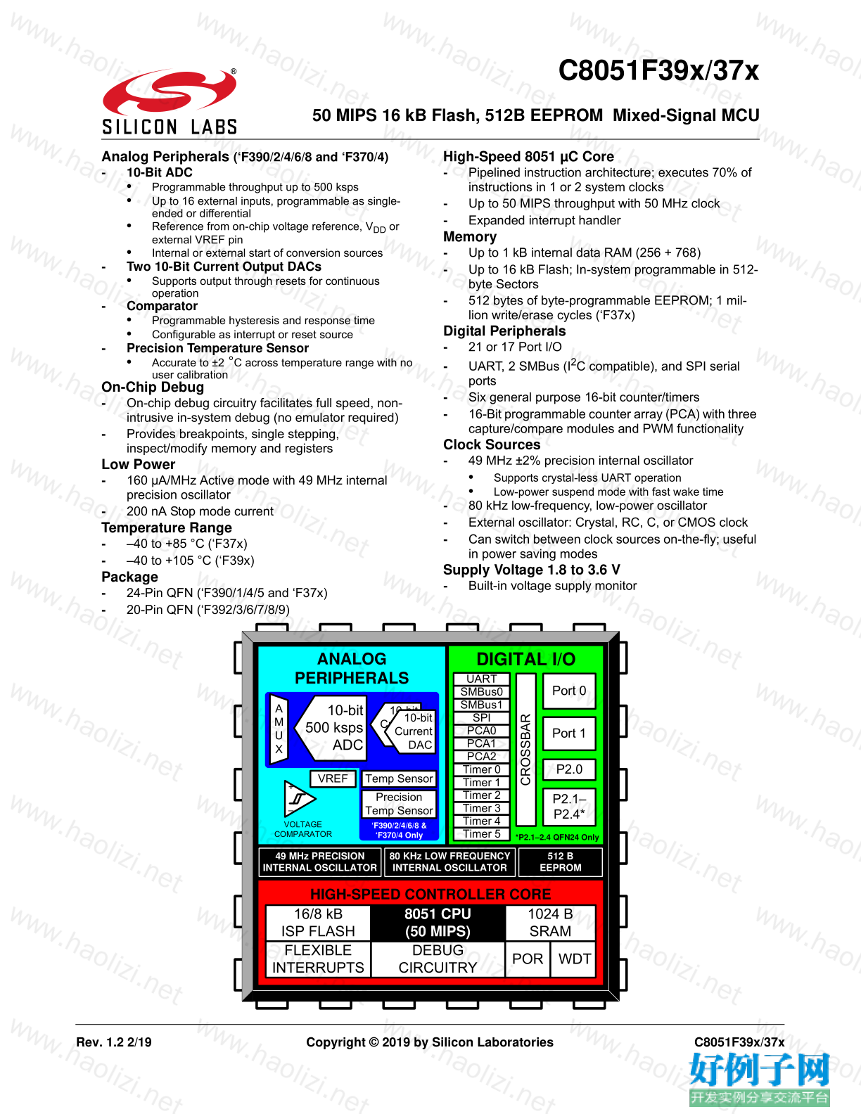
Figure 1.1. C8051F392/3/6/7/8/9 Block Diagram .................................................... 18
Figure 1.2. C8051F390/1/4/5 Block Diagram .......................................................... 18
Figure 1.3. C8051F370/1/4/5 Block Diagram .......................................................... 19
Figure 4.1. C8051F392/3/6/7/8/9 QFN-20 Pinout Diagram (Top View) ................... 25
Figure 4.2. C8051F390/1/4/5 Pinout Diagram (Top View) ...................................... 26
Figure 4.3. C8051F370/1/4/5 Pinout Diagram (Top View) ...................................... 27
Figure 5.1. QFN-20 Package Drawing .................................................................... 28
Figure 5.2. QFN-20 Recommended PCB Land Pattern .......................................... 29
Figure 6.1. QFN-24 Package Drawing .................................................................... 30
Figure 6.2. QFN-24 Recommended PCB Land Pattern .......................................... 31
Figure 7.1. Normal Mode Digital Supply Current vs. Frequency ............................. 45
Figure 7.2. Idle Mode Digital Supply Current vs. Frequency ................................... 45
Figure 7.3. Precision Temperature Sensor Error vs. Temperature ......................... 46
Figure 9.1. ADC0 Functional Block Diagram ........................................................... 50
Figure 9.2. 10-Bit ADC Track and Conversion Example Timing ............................. 53
Figure 9.3. ADC0 Equivalent Input Circuits ............................................................. 54
Figure 9.4. ADC Window Compare Example: Right-Justified, Single-Ended Data . 60
Figure 9.5. ADC Window Compare Example: Left-Justified, Single-Ended Data .... 60
Figure 9.6. ADC0 Multiplexer Block Diagram .......................................................... 61
Figure 10.1. Temperature Sensor Transfer Function .............................................. 64
Figure 10.2. Temperature Sensor Error with 1-Point Calibration at 0 °C ................ 65
Figure 11.1. IDA0 Functional Block Diagram .......................................................... 66
Figure 11.2. IDA1 Functional Block Diagram .......................................................... 67
Figure 11.3. IDA0 Data Word Mapping ................................................................... 68
Figure 12.1. Voltage Reference Functional Block Diagram ..................................... 73
Figure 14.1. Comparator0 Functional Block Diagram ............................................. 76
Figure 14.2. Comparator Hysteresis Plot ................................................................ 77
Figure 14.3. Comparator Input Multiplexer Block Diagram ...................................... 80
Figure 15.1. CIP-51 Block Diagram ......................................................................... 82
Figure 17.1. C8051F39x/37x Memory Map ............................................................. 93
Figure 17.2. Flash Program Memory Map ............................................................... 94
Figure 19.1. SFR Page Stack ................................................................................ 102
Figure 19.2. SFR Page Stack While Using SFR Page 0x0F To Access TS0CN .. 103
Figure 19.3. SFR Page Stack After SPI0 Interrupt Occurs .................................... 104
Figure 19.4. SFR Page Stack Upon PCA Interrupt Occurring During a SPI0 ISR 105
Figure 19.5. SFR Page Stack Upon Return from PCA0 Interrupt ......................... 106
Figure 19.6. SFR Page Stack Upon Return From SPI0 Interrupt .......................... 107
Figure 21.1. Security Byte Decoding ..................................................................... 133
Figure 22.1. Slave Address Byte Definition ........................................................... 141
Figure 22.2. Write Operation (Single Byte) ............................................................ 142
Figure 22.3. Write Operation (Multiple Bytes) ....................................................... 142
Figure 22.4. Current Address Read Operation (Single Byte) ................................ 143
Figure 22.5. Current Address Read Operation (Multiple Bytes) ............................ 144
Figure 22.6. Selective Address Read (Single Byte) .............................................. 145
Figure 22.7. Selective Address Read (Multiple Bytes) .......................................... 146
C8051F39x/37x
Rev. 1.2 9
Figure 23.1. CRC0 Block Diagram ........................................................................ 147
Figure 23.2. Bit Reverse Register ......................................................................... 149
Figure 24.1. Reset Sources ................................................................................... 155
Figure 24.2. Power-On and VDD Monitor Reset Timing ....................................... 156
Figure 26.1. Oscillator Options .............................................................................. 164
Figure 26.2. External Crystal Example .................................................................. 170
Figure 27.1. Port I/O Functional Block Diagram .................................................... 173
Figure 27.2. Port I/O Cell Block Diagram .............................................................. 174
Figure 27.3. Crossbar Priority Decoder - Possible Pin Assignments .................... 178
Figure 27.4. Crossbar Priority Decoder Example .................................................. 179
Figure 28.1. SMBus0 Block Diagram .................................................................... 192
Figure 28.2. Typical SMBus Configuration ............................................................ 193
Figure 28.3. SMBus Transaction ........................................................................... 194
Figure 28.4. Typical SMBus SCL Generation ........................................................ 196
Figure 28.5. Typical Master Write Sequence ........................................................ 211
Figure 28.6. Typical Master Read Sequence ........................................................ 212
Figure 28.7. Typical Slave Write Sequence .......................................................... 213
Figure 28.8. Typical Slave Read Sequence .......................................................... 214
Figure 29.1. UART0 Block Diagram ...................................................................... 220
Figure 29.2. UART0 Baud Rate Logic ................................................................... 221
Figure 29.3. UART Interconnect Diagram ............................................................. 222
Figure 29.4. 8-Bit UART Timing Diagram .............................................................. 222
Figure 29.5. 9-Bit UART Timing Diagram .............................................................. 223
Figure 29.6. UART Multi-Processor Mode Interconnect Diagram ......................... 224
Figure 30.1. SPI Block Diagram ............................................................................ 228
Figure 30.2. Multiple-Master Mode Connection Diagram ...................................... 230
Figure 30.3. 3-Wire Single Master and 3-Wire Single Slave Mode Connection Diagram
231
Figure 30.4. 4-Wire Single Master Mode and 4-Wire Slave Mode Connection Diagram
231
Figure 30.5. Master Mode Data/Clock Timing ....................................................... 233
Figure 30.6. Slave Mode Data/Clock Timing (CKPHA = 0) ................................... 233
Figure 30.7. Slave Mode Data/Clock Timing (CKPHA = 1) ................................... 234
Figure 30.8. SPI Master Timing (CKPHA = 0) ....................................................... 238
Figure 30.9. SPI Master Timing (CKPHA = 1) ....................................................... 239
Figure 30.10. SPI Slave Timing (CKPHA = 0) ....................................................... 239
Figure 30.11. SPI Slave Timing (CKPHA = 1) ....................................................... 240
Figure 31.1. T0 Mode 0 Block Diagram ................................................................. 246
Figure 31.2. T0 Mode 2 Block Diagram ................................................................. 247
Figure 31.3. T0 Mode 3 Block Diagram ................................................................. 248
Figure 31.4. Timer 2 16-Bit Mode Block Diagram ................................................. 253
Figure 31.5. Timer 2 8-Bit Mode Block Diagram ................................................... 254
Figure 31.6. Timer 2 Low-Frequency Oscillation Capture Mode Block Diagram ... 255
Figure 31.7. Timer 3 16-Bit Mode Block Diagram ................................................. 259
Figure 31.8. Timer 3 8-Bit Mode Block Diagram ................................................... 260
C8051F39x/37x
10 Rev. 1.2
Figure 31.9. Timer 3 Low-Frequency Oscillation Capture Mode Block Diagram ... 261
Figure 31.10. Timer 4 16-Bit Mode Block Diagram ............................................... 265
Figure 31.11. Timer 4 8-Bit Mode Block Diagram ................................................. 266
Figure 31.12. Timer 5 16-Bit Mode Block Diagram ............................................... 270
Figure 31.13. Timer 5 8-Bit Mode Block Diagram ................................................. 271
Figure 32.1. PCA Block Diagram ........................................................................... 275
Figure 32.2. PCA Counter/Timer Block Diagram ................................................... 276
Figure 32.3. PCA Interrupt Block Diagram ............................................................ 277
Figure 32.4. PCA Capture Mode Diagram ............................................................. 279
Figure 32.5. PCA Software Timer Mode Diagram ................................................. 280
Figure 32.6. PCA High-Speed Output Mode Diagram ........................................... 281
Figure 32.7. PCA Frequency Output Mode ........................................................... 282
Figure 32.8. PCA 8-Bit PWM Mode Diagram ........................................................ 283
Figure 32.9. PCA 9, 10 and 11-Bit PWM Mode Diagram ...................................... 284
Figure 32.10. PCA 16-Bit PWM Mode ................................................................... 285
Figure 32.11. PCA Module 2 with Watchdog Timer Enabled ................................ 286
Figure 32.12. Comparator Clear Function Diagram .............................................. 288
Figure 32.13. CEXn with CPCEn = 1, CPCPOL = 0 .............................................. 288
Figure 32.14. CEXn with CPCEn = 1, CPCPOL = 1 .............................................. 289
Figure 32.15. CEXn with CPCEn = 1, CPCPOL = 0 .............................................. 289
Figure 32.16. CEXn with CPCEn = 1, CPCPOL = 1 .............................................. 289
Figure 33.1. Typical C2 Pin Sharing ...................................................................... 300
C8051F39x/37x
Rev. 1.2 11
Table 2.1. Product Selection Guide ......................................................................... 20
Table 3.1. C8051F33x Replacement Part Numbers ................................................ 21
Table 4.1. Pin Definitions for the C8051F39x/37x ................................................... 22
Table 5.1. QFN-20 Package Dimensions ................................................................ 28
Table 5.2. QFN-20 PCB Land Pattern Dimensions ................................................. 29
Table 6.1. QFN-24 Package Dimensions ................................................................ 30
Table 6.2. QFN-24 PCB Land Pattern Dimensions ................................................. 31
Table 7.1. Absolute Maximum Ratings .................................................................... 32
Table 7.2. Global Electrical Characteristics ............................................................. 33
Table 7.3. Port I/O DC Electrical Characteristics ..................................................... 35
Table 7.4. Reset Electrical Characteristics .............................................................. 36
Table 7.5. Flash Electrical Characteristics .............................................................. 37
Table 7.6. EEPROM Electrical Characteristics ........................................................ 37
Table 7.7. Internal High-Frequency Oscillator Electrical Characteristics ................. 38
Table 7.8. Internal Low-Frequency Oscillator Electrical Characteristics ................. 38
Table 7.9. Internal Low-Power Oscillator Electrical Characteristics ........................ 38
Table 7.10. ADC0 Electrical Characteristics ............................................................ 39
Table 7.11. ADC Temperature Sensor Electrical Characteristics ............................ 40
Table 7.12. Precision Temperature Sensor Electrical Characteristics .................... 40
Table 7.13. Voltage Reference Electrical Characteristics ....................................... 41
Table 7.14. Voltage Regulator Electrical Characteristics ........................................ 41
Table 7.15. IDAC Electrical Characteristics ............................................................. 42
Table 7.16. Comparator Electrical Characteristics .................................................. 43
Table 8.1. Example Temperature Values in TS0DATH:TS0DATL .......................... 47
Table 15.1. CIP-51 Instruction Set Summary .......................................................... 84
Table 19.1. SFR Page Stack ................................................................................. 101
Table 19.2. Special Function Register (SFR) Memory Map .................................. 111
Table 19.3. Special Function Registers ................................................................. 112
Table 20.1. Configurable Interrupt Priority Decoding ............................................ 118
Table 20.2. Interrupt Summary .............................................................................. 119
Table 21.1. Flash Security Summary .................................................................... 133
Table 23.1. Example 16-bit CRC Outputs ............................................................. 148
Table 27.1. Port I/O Assignment for Analog Functions ......................................... 175
Table 27.2. Port I/O Assignment for Digital Functions ........................................... 176
Table 27.3. Port I/O Assignment for External Event Trigger Functions ................. 177
Table 28.1. SMBus Clock Source Selection .......................................................... 196
Table 28.2. Minimum SDA Setup and Hold Times ................................................ 197
Table 28.3. Sources for Hardware Changes to SMBnCN ..................................... 204
Table 28.4. Hardware Address Recognition Examples (EHACK = 1) ................... 205
Table 28.5. SMBus Status Decoding: Hardware ACK Disabled (EHACK = 0) ...... 215
Table 28.6. SMBus Status Decoding: Hardware ACK Enabled (EHACK = 1) ...... 217
Table 29.1. Timer Settings for Standard Baud Rates
Using The Internal 49 MHz Oscillator ................................................. 227
Table 29.2. Timer Settings for Standard Baud Rates
Using an External 22.1184 MHz Oscillator ......................................... 227
C8051F39x/37x
12 Rev. 1.2
Table 30.1. SPI Slave Timing Parameters ............................................................ 241
Table 32.1. PCA Timebase Input Options ............................................................. 276
Table 32.2. PCA0CPM and PCA0PWM Bit Settings for PCA Capture/Compare Mod-
ules ..................................................................................................... 278
Table 32.3. Watchdog Timer Timeout Intervals1 ................................................... 287
小贴士
感谢您为本站写下的评论,您的评论对其它用户来说具有重要的参考价值,所以请认真填写。
- 类似“顶”、“沙发”之类没有营养的文字,对勤劳贡献的楼主来说是令人沮丧的反馈信息。
- 相信您也不想看到一排文字/表情墙,所以请不要反馈意义不大的重复字符,也请尽量不要纯表情的回复。
- 提问之前请再仔细看一遍楼主的说明,或许是您遗漏了。
- 请勿到处挖坑绊人、招贴广告。既占空间让人厌烦,又没人会搭理,于人于己都无利。
关于好例子网
本站旨在为广大IT学习爱好者提供一个非营利性互相学习交流分享平台。本站所有资源都可以被免费获取学习研究。本站资源来自网友分享,对搜索内容的合法性不具有预见性、识别性、控制性,仅供学习研究,请务必在下载后24小时内给予删除,不得用于其他任何用途,否则后果自负。基于互联网的特殊性,平台无法对用户传输的作品、信息、内容的权属或合法性、安全性、合规性、真实性、科学性、完整权、有效性等进行实质审查;无论平台是否已进行审查,用户均应自行承担因其传输的作品、信息、内容而可能或已经产生的侵权或权属纠纷等法律责任。本站所有资源不代表本站的观点或立场,基于网友分享,根据中国法律《信息网络传播权保护条例》第二十二与二十三条之规定,若资源存在侵权或相关问题请联系本站客服人员,点此联系我们。关于更多版权及免责申明参见 版权及免责申明

网友评论
我要评论