
介绍
2026世界杯买球竞猜app官方最新版1.1.6是一款让你爱不释手的地方麻将游戏。它融合了经典麻将玩法与创新元素,带给玩家全新的游戏体验。无论是休闲娱乐还是挑战高手,都能在这个游戏中找到乐趣。
1、掌握牌型要领,了解各种胡牌规则,灵活运用策略获取胜利。
2、善用分析技巧,观察对手牌型,抓住机会打出致命一击。
3、注意手中牌的变化,灵活调整打法,应对不同局面。
4、善于思考,把握好进攻时机,稳扎稳打取得优势。
5、合理利用道具,增强自身实力,成为麻将界的一匹黑马。
1、创新的胡牌规则,让游戏更具挑战性和趣味性。
2、特色模式丰富多样,满足不同玩家的需求,让游戏更加精彩。
3、个性的任务系统,挑战各种难度,收获丰厚奖励。
4、丰富的活动内容,让玩家感受到游戏的无限乐趣。
5、社交互动功能,与好友组队对战,体验更多乐趣。
1、精致逼真的游戏场景,让玩家仿佛置身于真实的麻将室。
2、细腻流畅的操作体验,让玩家享受畅快淋漓的游戏感受。
3、华丽炫酷的特效设计,为游戏增添了不少视觉盛宴。
4、多样化的角色造型,个性鲜明,让玩家眼前一亮。
5、丰富的场景氛围,让玩家感受到不同的游戏氛围。
1、与其他玩家实时对战,体验激情四射的竞技乐趣。
2、匹配系统智能高效,让你随时随地找到对手展开对决。
3、多样化的战斗模式,让你尽情展现自己的麻将技艺。
4、激烈的竞争氛围,挑战更高的段位,成为真正的麻将高手。
5、丰富的奖励系统,为胜利加油助威,让你事半功倍。
1、快节奏的游戏节奏,让你感受到无与伦比的刺激。
2、流畅的操作体验,让你在瞬息万变中游刃有余。
3、紧张刺激的对局,让你时刻保持警觉,全神贯注。
4、简洁明了的界面设计,让你一目了然,畅快玩耍。
5、快速匹配系统,让你秒进游戏,随时随地畅快玩耍。
应用信息
相关资讯
更多 +相关下载
更多 +相关合集
更多 +
上班族手游
不再是枯燥的上班路!上班族手游合集带你开启别样游戏新体验!穿梭于繁忙的都市,你将...
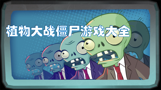
植物大战僵尸游戏大全
植物大战僵尸游戏大全汇集了一系列植物与僵尸的疯狂对决,让你体验截然不同的游戏版本...

跑酷单机游戏
欢迎来到极速冒险乐园!这里有一款超级炫酷的合集,汇集了一系列跑酷单机游戏。在这个...
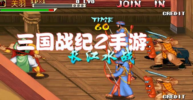
三国战纪2手游
准备好迎接三国风云了吗?三国战纪2手游合集横空出世!这是一场史诗级的战斗,在这个...
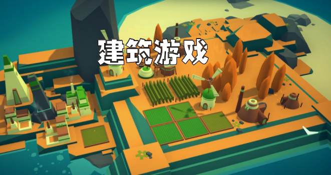
建筑游戏
哟,各位城市规划师!这里是建筑游戏的超级合集,一场让你发挥想象力、畅游建筑世界的...

角色扮演类游戏
角色扮演类游戏合集,探索无限可能的游戏世界!在这个合集中,你将发现多款游戏,每一...
最新更新