
实例介绍
【实例简介】Motorola_MVME5100_Manual.pdf
【实例截图】

【核心代码】
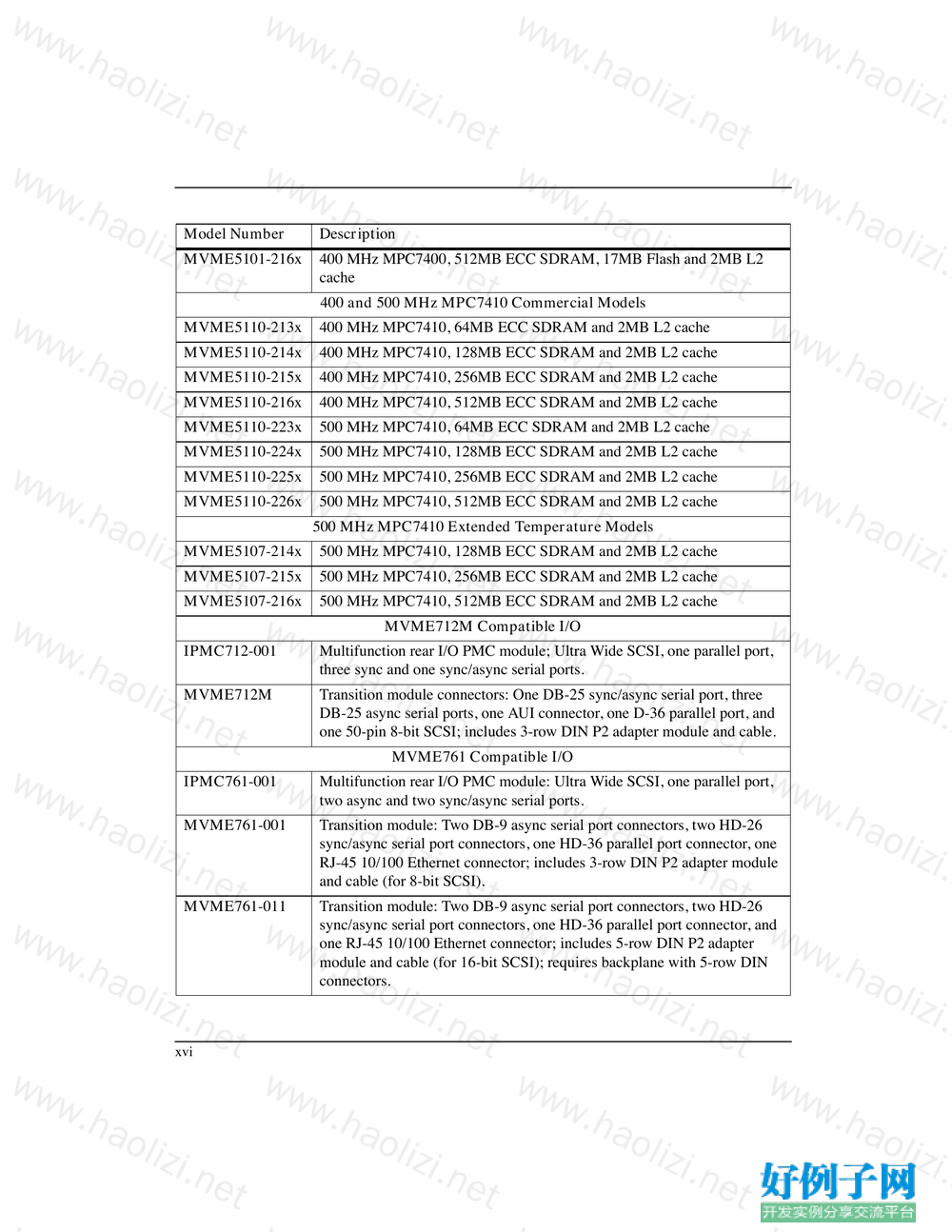
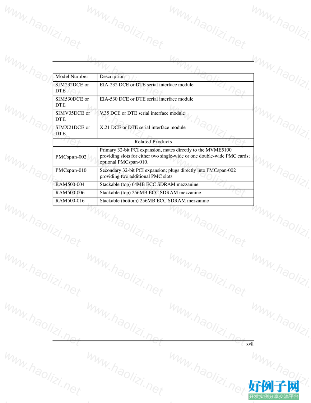
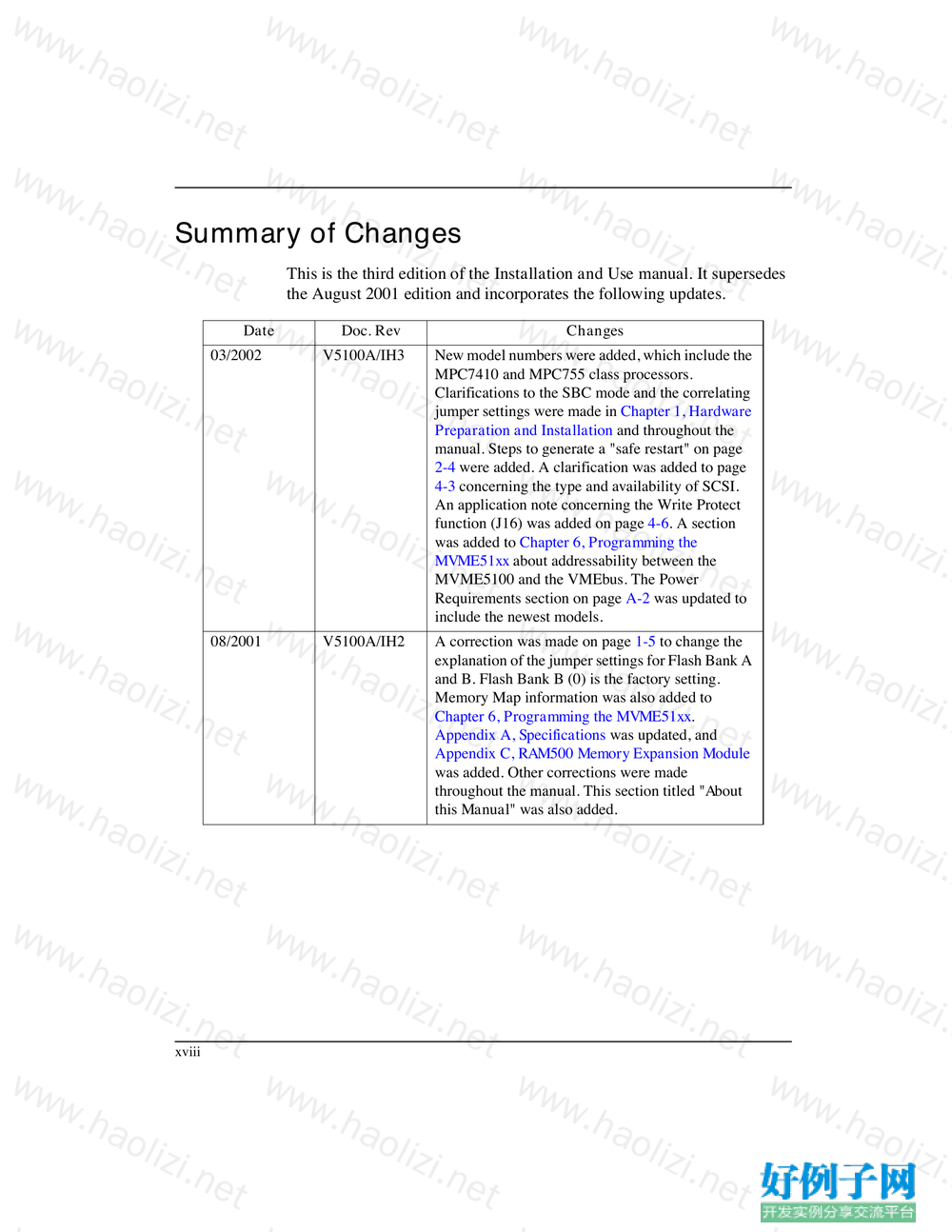
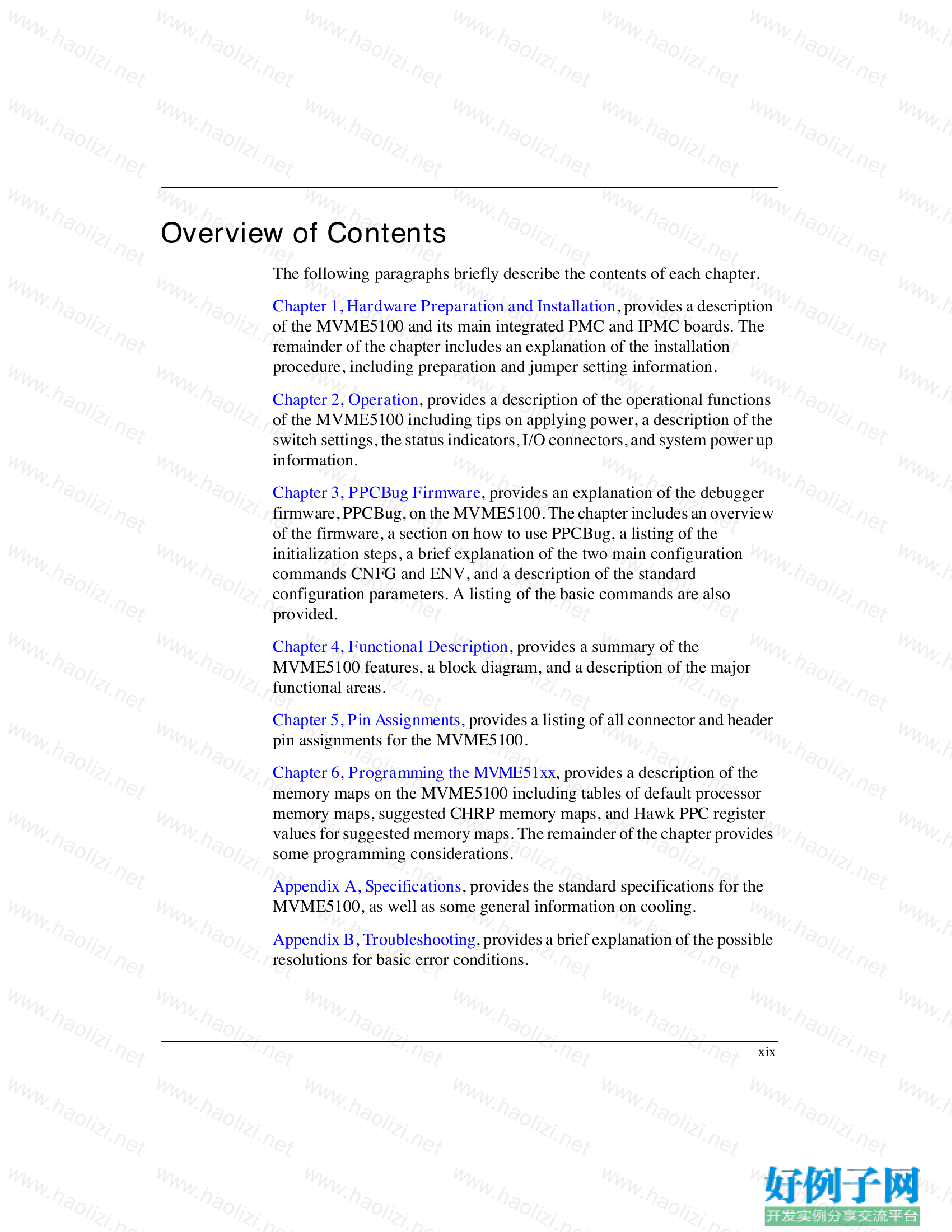
Contents
About This Manual
Summary of Changes...............................................................................................xviii
Overview of Contents ................................................................................................xix
Comments and Suggestions ........................................................................................xx
Conventions Used in This Manual.............................................................................xxi
Terminology........................................................................................................xxi
CHAPTER 1 Hardware Preparation and Installation
Introduction................................................................................................................1-1
Getting Started ...........................................................................................................1-1
Overview and Equipment Requirements ............................................................1-1
Unpacking Instructions .......................................................................................1-2
Preparation .................................................................................................................1-3
Hardware Configuration .....................................................................................1-3
Jumper Settings...................................................................................................1-5
PMC/SBC Mode Selection..........................................................................1-5
System Considerations........................................................................................1-7
Installation..................................................................................................................1-8
PMC Modules...................................................................................................1-10
Primary PMCspan.............................................................................................1-12
Secondary PMCspan.........................................................................................1-14
MVME5100 ......................................................................................................1-16
CHAPTER 2 Operation
Introduction................................................................................................................2-1
Switches and Indicators .............................................................................................2-1
ABT/RST Switch................................................................................................2-1
Abort Function.............................................................................................2-1
Reset Function .............................................................................................2-2
Safe Restart..................................................................................................2-2
Status Indicators..................................................................................................2-3
RST Indicator (DS1)....................................................................................2-3
CPU Indicator (DS2) ...................................................................................2-3
Connectors ..........................................................................................................2-3
viii
10/100BASET Ports.................................................................................... 2-3
DEBUG Port ............................................................................................... 2-4
System Power-up ....................................................................................................... 2-4
Initialization Process .......................................................................................... 2-4
CHAPTER 3 PPCBug Firmware
Introduction ............................................................................................................... 3-1
PPCBug Overview..................................................................................................... 3-1
Implementation and Memory Requirements...................................................... 3-3
Using PPCBug........................................................................................................... 3-3
Hardware and Firmware Initialization................................................................ 3-4
Default Settings ......................................................................................................... 3-6
CNFG – Configure Board Information Block.................................................... 3-7
ENV – Set Environment..................................................................................... 3-7
Configuring the PPCBug Parameters.......................................................... 3-8
LED/Serial Startup Diagnostic Codes.............................................................. 3-16
Configuring the VMEbus Interface .................................................................. 3-17
Firmware Command Buffer ............................................................................. 3-21
Standard Commands................................................................................................ 3-22
Diagnostics ....................................................................................................... 3-26
CHAPTER 4 Functional Description
Introduction ............................................................................................................... 4-1
Features Summary ..................................................................................................... 4-1
Features Descriptions ................................................................................................ 4-3
General ............................................................................................................... 4-3
Processor ............................................................................................................ 4-5
System Memory Controller and PCI Host Bridge.............................................. 4-5
Memory .............................................................................................................. 4-5
Flash Memory ............................................................................................. 4-5
ECC SDRAM Memory ............................................................................... 4-6
P2 Input/Output (I/O) Modes ............................................................................. 4-7
Input/Output Interfaces....................................................................................... 4-7
Ethernet Interface ........................................................................................ 4-7
VMEbus Interface ....................................................................................... 4-8
Asynchronous Communications ................................................................. 4-8
Real-Time Clock & NVRAM & Watchdog Timer..................................... 4-8
Timers ......................................................................................................... 4-8
Interrupt Routing......................................................................................... 4-8
ix
IDSEL Routing ............................................................................................4-9
CHAPTER 5 Pin Assignments
Introduction................................................................................................................5-1
Summary.............................................................................................................5-1
Jumper Settings..........................................................................................................5-2
Connectors .................................................................................................................5-3
IPMC761 Connector (J3) Pin Assignments........................................................5-3
Memory Expansion Connector (J8) Pin Assignments........................................5-4
PCI Expansion Connector (J25) Pin Assignments .............................................5-8
PCI Mezzanine Card (PMC) Connectors..........................................................5-11
VMEbus Connectors P1 & P2 Pin Assignments (PMC mode) ........................5-24
VMEbus P1 & P2 Connector Pin Assignments (SBC Mode) ..........................5-26
10BaseT/100BaseTx Connector Pin Assignments ...........................................5-30
COM1 and COM2 Connector Pin Assignments...............................................5-31
CHAPTER 6 Programming the MVME51xx
Introduction................................................................................................................6-1
Memory Maps............................................................................................................6-1
Processor Bus Memory Map...............................................................................6-2
Default Processor Memory Map..................................................................6-2
Processor Memory Map...............................................................................6-3
PCI Memory Map........................................................................................6-4
VME Memory Map .....................................................................................6-5
PCI Local Bus Memory Map..............................................................................6-5
VMEbus Memory Map .......................................................................................6-5
Establishing Addressability on the VMEbus...............................................6-6
Programming Considerations.....................................................................................6-7
PCI Arbitration ...................................................................................................6-8
Interrupt Handling.............................................................................................6-10
DMA Channels .................................................................................................6-12
Sources of Reset................................................................................................6-12
Endian Issues ....................................................................................................6-14
Processor/Memory Domain.......................................................................6-14
PCI Domain ...............................................................................................6-14
VMEbus Domain.......................................................................................6-15
x
APPENDIX A Specifications
General Specifications .............................................................................................. A-1
Power Requirements................................................................................................. A-2
Cooling Requirements .............................................................................................. A-3
APPENDIX B Troubleshooting
Solving Startup Problems ......................................................................................... B-1
APPENDIX C RAM500 Memory Expansion Module
Overview................................................................................................................... C-1
Features..................................................................................................................... C-1
Functional Description ............................................................................................. C-2
RAM500 Description ........................................................................................ C-2
SROM................................................................................................................ C-5
Host Clock Logic............................................................................................... C-5
RAM500 Module Installation................................................................................... C-5
RAM500 Connectors................................................................................................ C-7
Bottom Side Memory Expansion Connector (P1)............................................. C-7
Top Side Memory Expansion Connector (J1) ................................................. C-10
RAM500 Programming Issues ............................................................................... C-12
Serial Presence Detect (SPD) Data ................................................................. C-13
APPENDIX D Related Documentation
Motorola Computer Group Documents.................................................................... D-1
Manufacturers’ Documents ...................................................................................... D-2
Related Specifications .............................................................................................. D-4
xi
List of Figures
Figure 1-1. MVME5100 Layout ................................................................................1-9
Figure 1-2. MVME5100 Installation and Removal From a VMEbus Chassis ........1-11
Figure 1-3. Typical PMC Module Placement on an MVME5100 ...........................1-11
Figure 1-4. PMCspan-002 Installation on an MVME5100 .....................................1-13
Figure 1-5. PMCspan-010 Installation on a PMCspan-002/MVME5100 ...............1-15
Figure 2-1. Boot-Up Sequence ..................................................................................2-5
Figure 4-1. MVME5100 Block Diagram...................................................................4-4
Figure 6-1. VMEbus Master Mapping.......................................................................6-9
Figure 6-2. MVME51xx Interrupt Architecture ......................................................6-11
Figure C-1. RAM500 Block Diagram .....................................................................C-4
Figure C-2. RAM500 Module Placement on MVME5100 .....................................C-6
好例子网口号:伸出你的我的手 — 分享!
小贴士
感谢您为本站写下的评论,您的评论对其它用户来说具有重要的参考价值,所以请认真填写。
- 类似“顶”、“沙发”之类没有营养的文字,对勤劳贡献的楼主来说是令人沮丧的反馈信息。
- 相信您也不想看到一排文字/表情墙,所以请不要反馈意义不大的重复字符,也请尽量不要纯表情的回复。
- 提问之前请再仔细看一遍楼主的说明,或许是您遗漏了。
- 请勿到处挖坑绊人、招贴广告。既占空间让人厌烦,又没人会搭理,于人于己都无利。
关于好例子网
本站旨在为广大IT学习爱好者提供一个非营利性互相学习交流分享平台。本站所有资源都可以被免费获取学习研究。本站资源来自网友分享,对搜索内容的合法性不具有预见性、识别性、控制性,仅供学习研究,请务必在下载后24小时内给予删除,不得用于其他任何用途,否则后果自负。基于互联网的特殊性,平台无法对用户传输的作品、信息、内容的权属或合法性、安全性、合规性、真实性、科学性、完整权、有效性等进行实质审查;无论平台是否已进行审查,用户均应自行承担因其传输的作品、信息、内容而可能或已经产生的侵权或权属纠纷等法律责任。本站所有资源不代表本站的观点或立场,基于网友分享,根据中国法律《信息网络传播权保护条例》第二十二与二十三条之规定,若资源存在侵权或相关问题请联系本站客服人员,点此联系我们。关于更多版权及免责申明参见 版权及免责申明

网友评论
我要评论